llmda newsletter ad (2)

Will AMD Crash Intel’s $300M Ultrabook Party?

Will AMD Crash Intel’s $300M Ultrabook Party?
by Ed McKernan on 08-14-2011 at 7:00 am

Let’s face it, the ships are burning in the harbor and there is only one way out of here for AMD. It needs to crash Intel’s exclusive $300M Ultrabook Party in order to grab a slice of the future, more profitable PC market.

Intel Capital Creates $300 Million Ultrabook Fund
Continue reading “Will AMD Crash Intel’s $300M Ultrabook Party?”


ANSYS/Apache

ANSYS/Apache
by Paul McLellan on 08-13-2011 at 2:43 pm

Last week I met with Andrew Yang, erstwhile CEO of Apache Design Systems and now formally President of Apache Design Inc, a wholly owned subsidiary of ANSYS. The merger formally closed at the start of the month. Within ANSYS Apache is positioned as Chip-aware System-level Engineering Simulation. ANSYS is pretty much completely focused on different kinds of simulation and on simulation-driven product development.

ANSYS will keep Apache as a subsidiary and, in particular, the Apache name (and presumably the names of its products) will not be going away. The system design challenges that Apache is addressing fall into four main areas: power integrity, signal integrity, thermal/mechanical-stress integrity and electro-magnetic interference integrity. Most of these are dominated by various aspects of switching power.

Anyone who has been through many mergers knows just how much time can be burned up in dealing with overlapping products, so this merger has it easy. There is no overlap at all. However, there is plenty of customer overlap.

ANSYS is a very different company from even a big EDA company. It makes about 1/3 of its money on mechanical, 1/3 on fluid dynamics and 1/3 on electronics (now including Apache of course). Andrew was rightly proud that all 20 of the top 20 semiconductor companies used Apache, with over 100 total customers. ANSYS has over 40,000 customers (including 97 of the Fortune 100).

In some ways, EDA is an easy industry: look at the semiconductor roadmap, find some effect that is currently second or third order but which will become important, and produce a solution that is ready just when designers need it. However, getting the timing right is very difficult and more companies/products fail from being too early than being too late. Apache has done a superb job of getting this timing just right so that as power and noise became more important they had the best (or sometimes only) products to perform the analysis.

For example, a few years ago they decided that it was no longer possible to just look at the chip, they needed simultaneous analysis of chip, package and board. They acquired Optimum to jump start the package and board side of things and built a whole infrastructure for creating power models for chips and being able to analyze what came to be called chip-package-system (CPS). With the coming of 3D chips and through-silicon vias (TSVs) there are even more challenges in this area, especially the thermal issues once many die are stacked and it is hard to get the heat out.

Based on that track record, I asked Andrew what is next. What second order effects are we going to have to start to worry about. He reckons that it is quantum effects and the impact on reliability. The margin on transistor thresholds is going away as voltages continue to decrease. Leakage will get even more out of control (and since leakage also increases with temperature there are very real possibilities of thermal runaway). It is going to get very hard to guarantee that a chip will work correctly in the system and that it will be possible to manufacture.

ANSYS (with Apache) is extending chip-package-system to include other parts of the system such as multi-physics simulation. In many areas, most obviously automotive and aerospace, electronics is intimately tied in with mechanical and simulation-driven product development needs to combine these previously independent areas.

Note: You must be logged in to read/write comments


Current State of Tablet Products

Current State of Tablet Products
by Daniel Nenni on 08-12-2011 at 12:57 pm

attachment

Tablets are hot items these days. There is exuberance about the speed of application processors, size of the internal memory, capabilities of the operating systems, WiFi or 3G/4G connectivity, quality of the display, cameras megapixels, battery life, tablet weight, etc. All of these features are very important, no question about that; how else could one compare one product to the other? But let us step back for a moment and look at the bigger picture and see if there are some common threads.

I believe several trends deserve our attention and should be spelled out. These are: the proliferation of the operating systems, proliferation of the form factors, and price point.

The proliferation of the operating systems, as shown in Table 1, is evident. This is not exactly a testament to a harmonization effort; it looks more like the Wild West, where everyone is trying individually to position themselves as a serious contender by getting consumer attention in this newly created market segment without much consideration for standardization. There are currently six major operating systems (Android, iOS, WP7, QNX OS, WebOS, and MeeGo) jogging for the front position, and a few more in the works, recently announced by several companies; and every single one is creating its own ecosystem and applications.

The proliferation of different form factors (anything from 5” to 10” displays), as shown in Table 2, is another characteristic of the current products, suggesting that the entire tablet market segment is in a state of ‘soul searching,’ trying to find out what the customers prefer. This is not necessarily a bad thing, but it suggests that tablets as products are indeed in their infancy and significant transformations of these products should be expected in the next couple of years before consumers cast their final judgment.

Finally, here is the third important point related to the current tablet products. The selling price of the tablets from all major manufacturers is still high – clustering around $500. Thus, it should not come as a surprise that the second highest selling product after the iPad2 tablet in the first quarter of 2011 was Barnes and Noble’s 7 inch Nook Color priced at $250, according to the report from DigiTimes. This trend is expected to continue for the rest of the year. A price point of $250 is half that of the rest of the crowd, and certainly represents one of the best values.

Here is the interesting part. Nook Color is not the most capable tablet but it is a solid performer. It runs the Froyo (Android 2.2) operating system tuned by Barnes and Nobel for selling books and magazines. The application processor is TI’s OMAP 3621 (the same line of OMAP 3 processors that is found in Motorola’s smartphones Droid X and Droid2). This is a single core application processor, not exactly the top of the line as is the dual core Tegra 2 from nVidia (which is found in the top tier tablets). And yet, Nook Color, the modest performer that it is, still outsells all other feature-rich android tablets.

Table 1: Operating Systems for Tablets and Smartphones

Company Operating Systems Product Top Tier OEMs
(manufacturers of smartphones and tablets)
1. Google Android 2.2/2.3 (Froyo/Gingerbread) smartphones, tablets Google, MOT, Samsung, HTC, LG, Sony Ericsson, Dell, ZTE, Huawei, Lenovo, Asus, NEC, Sanyo, Sharp
Android 3.1 (Honeycomb) tablets MOT, Samsung, HTC, LG, Sony, Dell, ZTE, Huawei, Lenovo, Asus, Sharp
Android 2.4 (or 4x) (Ice Cream Sandwich) smartphones, tablets Expected: Google, MOT, Samsung, HTC, LG, Sony, Dell, ZTE, Huawei, Lenovo, Acer, Asus, NEC, Sanyo, Sharp
2. Apple Apple iOS 4 iPhone, iPad Apple
Apple iOS 5 iPhone, iPad Apple
3. BlackBerry QNX Neutrino OS tablets RIM
BlackBerry OS 6 smartphones RIM
BlackBerry OS 7 smartphones RIM
Blackberry Colt smartphones, tablets RIM
4. MSFT Windows WP7.1 (Mango) smartphones, tablets Nokia, Samsung, HTC, LG, Sony Ericsson, Dell, ZTE, Huawei, Lenovo, Asus, MSI
WP8 smartphones, tablets Expected: Nokia, MOT, Samsung, HTC, LG, Sony Ericsson, Dell, ZTE, Huawei, Lenovo, Asus, MSI
5. HP webOS 2.0 smartphones, tablets HP
webOS 3.0 tablets HP
6. Intel MeeGo 1.1 smartphones, tablets Intel, Acer, Lenovo. MSI
7. Nokia Symbian smartphones Nokia

Note: Symbian is listed here since there still will be a number of legacy smartphones from Nokia

But there is an additional reason for the popularity of Nook Color. Once launched, it got help from the Android cell phone and tablet community of developers that developed the modded version of Google Android called CM7 specifically for Nook Color, all in an attempt to enrich this product. In collaboration with another group, XDA Developers, together they created stable software. This software is basically Android 2.3.4 (Gingerbread) that can be booted to Nook Color via a micro SD card loaded with the software. The end result is that, Nook Color can operate in dual mode, either using Froyo that came with the original device from Barnes & Nobel, or the advanced Gingerbread operating system loaded on a micro SD card. One can purchase a preloaded 8, 16, or 32 GB micro SD card from n2a SD Cards via Amazon. In essence, all together you can get a full blown 7” tablet with the same capabilities as Samsung’s Galaxy Tab for under $300. And that is a real deal! This is a fine example of the importance that open source projects can play in shaping a product and a market.

Table 2: Tablet Form Factor

Screen Size Major OEMs Note
5 Inch Dell, Archos, Samsung, Sony Sony-5.5 ” dual screen tablet
7 Inch Samsung, Barnes & Noble, Dell, HTC, RIM, Acer, ViewSonic, Huawei, HP, Sharp, MSI, Mot Nook Color at $250; ViewSonic at $250
8 Inch Vizio, Archos Vizio at $299
9 Inch LG, Pandigital, Archos, Samsung, Amazon Includes 8.9″ size
10 Inch iPad, Mot, Samsung, Dell, HP, MSI, Acer, Archos, HTC, Sony Size from 9.7″ to 10.1″

Note: Listed OEMs are shown as examples only

The market success of the Nook Color has not gone unnoticed. Other tablet manufacturers are getting the message about the critical role of tablet price for market penetration. ViewSonic has announced a new lower $250 price for its 7” tablet, and so did Vizio for its 8” tablet, dropping the price to $299. The latest company to follow the trend is HP, dropping the price for its 16 GB 10” TouchPad that runs webOS 3.0 to $399. Consumers will certainly love this trend.

Lj. Ristic, Managing Director, Mobile Markets, Petrov Group, Palo Alto, CA

<script type=”text/javascript” src=”http://platform.linkedin.com/in.js”></script><script type=”in/share” data-counter=”right”></script>



nVidia: "30 Days From Going Out of Business"

nVidia: "30 Days From Going Out of Business"
by Ed McKernan on 08-11-2011 at 9:36 pm

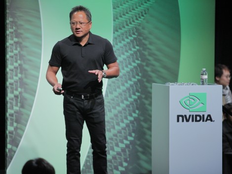
Jen Hsun Huang, the CEO of nVidia, has a phrase he often repeats to his employees: “We are 30 days from going out of business.” With product cycles as short as 6 months, the troops are on a constant march to revenue. The earnings conference call on August 11th highlighted two critical pieces of information. First, is the success that they are having in growing their PC graphics revenue despite the Sandy Bridge onslaught. Second, and more important, there is an internal and now a publicly articulated goal that they will reach a $1B revenue run rate for Tegra in 2012.

As outlined in an earlier Semiwiki blog titled “Intel’s Barbed Wire Fence Strategy”
http://www.semiwiki.com/forum/content/651-intel-s-barbed-wire-strategy.html Intel is in the business of expanding its fence lines. Their current target is nVidia’s graphics business. It represents not only additional revenue but also the ability to deny nVidia the funds to develop Tegra chips that will be used competitively in Smartphones and Tablets using Android as well as some Windows 8 mobiles.

All this may sound like Intel is the one to be most at risk to market share loss in 2012, especially with the launch of Windows 8 but, as a matter of fact, it is the other way around. First recognize that nVidia has finally returned to its peak run rate of $1B a quarter that they reached in 2007. Meanwhile, Intel is on track to do $55B in revenue this year or nearly 50% higher than 2007. Intel has the additional profits to crank out more designs targeting more segments. But there are clouds of uncertainty.

Windows 8, as understood by most people, unlocks the whole PC market to ARM based processors. Untrue! To get Win 8 to be light on its feet – meaning small memory footprint and fast boot/resume – Microsoft had to make compromises. First and foremost, Microsoft had to limit the hardware ecosystem. A closed system with support for fewer I/O devices makes life easier. No more Swiss Army Knife. How well will the Win 8 mobile run? We won’t know until it ships. The reduced hardware ecosystem should be fine for tablet – but a “clamshell” design is open to interpretation. Are they reduced netbooks?

Intel’s challenge is much different than nVidia’s but still attainable. Back in May, at their Analyst Meeting, Paul Otellini announced they were dropping their Thermal Design Point (TDP) for processors from 35W to 17W. We now know what drove them to this decision, or better yet, who drove them to this decision.

A story broke yesterday in the Wall St. Journal where it was noted that Apple informed Intel that it better drastically slash its power consumption or risk losing Apple’s business. As an Intel exec said, “It was a real wake up call to us.” For more on the story – follow the link:

http://blogs.wsj.com/digits/2011/08/10/intel-sets-300-million-fund-to-spur-ultrabooks/

As I mentioned in an earlier blog, the MAC Air is driving the mobile market. It uses Intel ULV processors that have a TDP of 17W (50% lower than regular Intel mobile Sandy Bridge CPUs) and sells for a minimum of $220. The price of the CPU is based on the yield they get per wafer. In this case <50%. Intel needs to get to 7W ideally to make Apple happy in the near term. And they need to offer an entry-level price closer to $75 – so Apple can take MAC Air to $799 thereby sucking the oxygen out of the notebook PC market. This is where I believe Intel will be one year from now with the 22nm Ivy Bridge ULV (A straight die shrink of Sandy Bridge at a similar MHz to today’s ULV). If this still seems high relative to ARM, it is, and Apple has probably informed Intel that they need a 3-5W TDP with Haswell as they go even more aggressive on a future MAC Air. Sound confusing? Consider this like two great armies rushing to the same spot at the front. Each has their own unique strengths and weaknesses. In the end – it is the market that lies just a tad above Apple’s entry level $499 iPAD. Call it $499+1. Note: You must be logged in to read/write comments


Altera and Xilinx Eyeing 28nm FPGA Dominance

Altera and Xilinx Eyeing 28nm FPGA Dominance
by Ed McKernan on 08-11-2011 at 7:00 am

28nm FPGAs are finally hitting the market and the next round in the battle between Altera and Xilinx is heating up. At 40nm, Altera beat Xilinx out the door by a year and as a consequence won a lot of new sockets in the high end Communications market. In the past year, Altera has closed the revenue and market share gap with Xilinx. This new round at 28nm looks to be much closer. However, the winner of the contest may come down to whom has the better eye – as in eye diagram.

Previously, I was a co-founder of Cswitch, a packet based FPGA startup that built the fastest FPGA in 90nm. It featured a new interconnect that could route 400Gb around the chip to be manipulated in special packet processing engines. It was an awesome chip that was suitable for 40G and 100G routers that would normally require 2 or 3 high end FPGAs. We were going after the 45% of the FPGA market tied to high $$$ wired and wireless communications. Alas we ran out of money after samples were delivered but before production started.

In the old days it was all about the tools – whoever has the best tools wins. More recently IP is playing a huge factor in who wins sockets as the engineers are looking to get their design done quickly and accurately. However, as you go up in performance and capability, it is the speed, number and quality of the Serdes that determines if you are even in the game to begin with. We were running 40 Serdes at 6.3G+ at Cswitch – today Xilinx and Altera are running up to 28G to support 100G/400G designs – Amazingly Fast. Altera and Xilinx want to get out of the gates quickly because they are first with the fastest Serdes (beating Broadcom and the NPU vendors). The prototype revenue alone is large as chips sell for $6K, $8K or $10K each. But Cisco, Alcatel, Huawei, Juniper, and others are looking to get product out quick with the latest 100G and 400G routers and switches to show their customers and perhaps do field trials.

Lately Xilinx and Altera are out promoting their Serdes heavily to convince engineers that they are ready.

Here’s Altera’s 28G Serdes Demo:

http://www.altera.com/education/webcasts/videos/videos-industry-first-28gbps-fpga.html?contactID=177581473&gwkey=EGIRI8TNBL

Here’s the Xilinx Serdes 28G Demo:

http://www.xilinx.com/technology/roadmap/28g-serial-transceiver-technology.htm

I am not an expert on Serdes but I am sure a few of our readers are and would be willing to share their thoughts on whether Xilinx and Altera have nailed it at 28nm. Who has the better eye and the least jitter? Let us know.


How Tektronix uses Hardware Configuration Management tools in an IC flow

How Tektronix uses Hardware Configuration Management tools in an IC flow
by Daniel Payne on 08-10-2011 at 5:49 pm

Last Monday I sat down with Grego Sanguinetti in Beaverton, Oregon at the campus of Tektronix to hear about how they design their ICs using EDA tools from multiple vendors.


Continue reading “How Tektronix uses Hardware Configuration Management tools in an IC flow”


Reducing SoC Power Consumption using Integrated Voltage Regulators

Reducing SoC Power Consumption using Integrated Voltage Regulators
by Daniel Nenni on 08-10-2011 at 5:00 pm

Last month I had the pleasure of meeting Mr Wonyoung Kim, a PhD candidate from Harvard University. Like many candidates, Wonyoung is shopping his thesis for capital in hopes of starting a semiconductor IP company. Here is a brief summary of the technology, please provide appropriate feedback and let’s see if we can get him some seed money:
Continue reading “Reducing SoC Power Consumption using Integrated Voltage Regulators”


Best EDA company for work life balance?

Best EDA company for work life balance?
by Daniel Payne on 08-10-2011 at 1:25 pm

What was the first EDA company name that came to your mind after reading that title?

At Forbes magazine they rated both Mentor Graphics and Synopsys in the top 25 best companies for work life balance.

That’s quite an honor for both Mentor and Synopsys so I can say that EDA dominated the list this year.

Here are some of the factors that give Mentor such an honor:

  • Corporate headquarters in Wilsonville, Oregon an affordable place to live (compared to Silicon Valley)
  • Five weeks of paid vacation per year (Flexible Time Off)
  • Medical benefits
  • Dental benefits
  • 401K plan with matching funds
  • Annual company picnic
  • Annual company party
  • Child care in Wilsonville from newborn thru Kindergarden
  • Gym with basketball court in Wilsonville
  • Perks for top employees (tickets to NBA, NHL, etc.)
  • Employee stock purchase plan with guaranteed 15% discount
  • Adoption program
  • Women can nurse their infants
  • Prepaid legal program

Here’s the list of the top 25 companies for work-life balance:
[LIST=1]

  • Nestle Purina PetCare
  • Mitre
  • SAS Institute
  • FactSet
  • United Space Alliance
  • Slalom Consulting
  • Facebook
  • Morningstar
  • Susquehanna International Group
  • Colgate-Palmolive
  • Mentor Graphics
  • Autodesk
  • Sheetz
  • Agilent Technologies
  • Turner Broadcasting
  • DuPont
  • Southwest Airlines
  • General Mills
  • Biogen Idec
  • Scottrade
  • Chevron
  • Synopsys
  • MTV Networks
  • Intuit
  • National Instruments

  • Yalta in EDA: but Synopsys ultra dominant in Interface IP territory…

    Yalta in EDA: but Synopsys ultra dominant in Interface IP territory…
    by Eric Esteve on 08-10-2011 at 10:32 am

    If Cadence is making money with large VIP port-folio, Synopsys has successfully deployed an acquisition strategy to build a large Design IP port-folio. Looking at these acquisitions will help understanding Synopsys positioning in the IP market. When they have started this acquisition campaign, back in 2002, their market share was a few % of a market weighting less than $1 Billion…

    The first acquisition was InSilicon in July 2002. Synopsys bought IP for interface standards such as USB, PCI, Ethernet, and 1394. This was their first step in the Interface, standard based, IP market and they keep playing in this segment, doing pretty well as they are now the undisputed leader as we will see further in this blog.

    Then they have acquired Cascade in October 2004. Cascade, was one of the very first companies involved in the new (at that time) PCI Express protocol. They plaid the game pretty well, their Controller IP being selected by the PCI-SIG as the reference system to be used for testing any new PCI Express system (IP, ASSP or board) during “plugfest”, in order to get the certification. Thus, CASCADE was were very well positioned to enjoy the first sales of PCIe IP, when you can charge for the license a price which is X3 or X4 that it will be a couple of years later! Even if Synopsys had already a design team developing a PCIe Controller (and PHY) IP, acquisition was a quick and efficient way to kill a dangerous competitor, and to jump start in this market with the positive image of an Innovator. At that time the PCI Express IP market, as reported by Gartner, was pretty small. Amazing to notice, three out the four companies ranked in the top 4, Rambus, ARM and Cadence have exited the market in the meantime (2007-2008). Rambus and ARM because it was not on line with their new business model. But Cadence came back in 2010 when they bought Denali, it’s too early to know what will be their success.

    In 2007, Synopsys was enjoying business growth –and good market share- in almost every segment of Interface IP: USB, PCIe, SATA, except Memory Controller (DDRn). This market segment was strongly dominated by Rambus and Denali, which make sense as both companies where involved for long time in development around DRAM. As the ASIC market was moving to a SoC market (ASIC + embedded core), the need to integrate a Memory Controller to interface with external DRAM, in a more and more complex manner, was pushing the DDRn Controller IP sales. Once again, Synopsys decided for the faster and easier (providing you have deep pocket) way: they bought Mosaid in July 2007 and get access to the DDRn Controller IP market, which was not so big at that time:

    In 2009 they were doing well in every segment of the Interface IP market, so the acquisition of the mixed-signal IP division of MIPS (in fact Chipidea bought in August 2007 for $147 million in cash!) in May 2009 for a mere $22 million was an opportunistic move. First, it brings a large port-folio of mixed signal IP (ADC, DAC and many more), allowing Synopsys to expand the penetration in the IP market, in a segment they have ignored so far. It was also a way to definitely kill any competition in the USB IP market, where they enjoyed already more than 60% market share and ChipIdea/MIPS 26%…

    Also to notice, the fact that Chipidea was involved in two recent if not emerging protocols: HDMI and MIPI, even if this was not the reason for buying. This acquisition was just the kind of opportunity you can’t miss, and the reason why MIPS accept such a discounted price had to do with the recession, but also with the fact they didn’t succeed in running a mixed signal IP product line, where every design-in is almost a redesign, completely at the opposite with processor core.

    So you could think that it was enough acquisitions. But the next important move on the chessboard came from cadence: they acquired Denali for $315M in May 2010! I am sure (even if I share no secret as I don’t really know it by fact) that Synopsys has to do with this pretty high price (a x7 multiple of Denali revenue), and that they have pushed up the bidding. Nevertheless, Denali was doing very well with DDRn Controller IP, and many analysts propose predictions above $100M for this IP segment. If you look for a way to expand your business by going in a place where you are not (Memory compilers and Libraries), and consolidate your share in DDRn Controller IP, then Virage Logic looks to be the right acquisition to do, and a smart way to answer to Cadence acquisition of Denali, is’n it? That was the last acquisition made by Synopsys, in June 2010. When you look at the DDRn Controller IP market figures for 2009, and when you know that the target was $10M for Virage Logic for 2010, you better understand it, even if adding a $40M to $50M yearly revenue coming from Memory Compilers and Libraries was also part of the equation, but the expected growth for these segments is almost null:

    So, acquisition after acquisition, Synopsys has built a wide port-folio including:

    and they have a dominant position in each product line. They have also acquired ARCprocessor core product line (through Virage Logic), and they clearly have a weak position here. Moreover, does Synopsys really want to compete with ARM core’s business? I am not sure, but we will see what will happen in the future…

    Eric Estevefrom IPnest(a lot more about Interface IP here)


    Speeding Verification of FPGA Prototype Boards

    Speeding Verification of FPGA Prototype Boards
    by Paul McLellan on 08-09-2011 at 5:42 pm

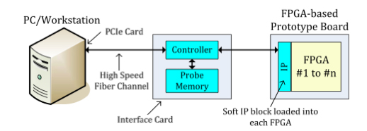
    It is no secret that SoC designs continue to increase in complexity and time-to-market windows are shrinking. While there is room for debate on just how big a fraction of SoC design effort goes on verification, there is no debating that it is a large part of the total. Simulation is increasingly too slow, especially when software has to be verified against the hardware. In some areas, formal techniques can be attractive but they are not universally applicable. One attractive approach is to use FPGAs to build a prototype of all or part of the SoC use this for verification. However, one big challenge is that synthesis, place and route for an SoC-sized FPGA can take as long as a day. It is impossible to observe every signal in a large SoC and so the SoC must be re-synthesized each time that a change is required in which signals need to be kept track of. Full re-creation of all the layout each time a change is made in the choice of signals is too slow. ProtoLink Probe Visualizer is a new approach to the problem. By understanding the placement and routing within the FPGA it is possible to make changes incrementally and almost instantaneously. With the addition of an interface containing probe memory, the data that it is possible to collect goes from 10s of signals for limited cycles, with a one day turnaround on changes to the signal list, to thousands of signals for millions of cycles, with a few minutes to update the list. The whitepaper is here.