Last month I had the pleasure of meeting Mr Wonyoung Kim, a PhD candidate from Harvard University. Like many candidates, Wonyoung is shopping his thesis for capital in hopes of starting a semiconductor IP company. Here is a brief summary of the technology, please provide appropriate feedback and let’s see if we can get him some seed money:

Dynamic voltage and frequency scaling (DVFS) is used in modern SoCs to save power by scaling both the voltage and frequency according to CPU demand. However, the effectiveness of current power management techniques are limited by the following.
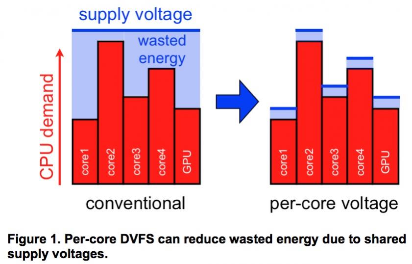
1) DVFS: shared voltage across multiple cores/IP blocks (Figure 1)
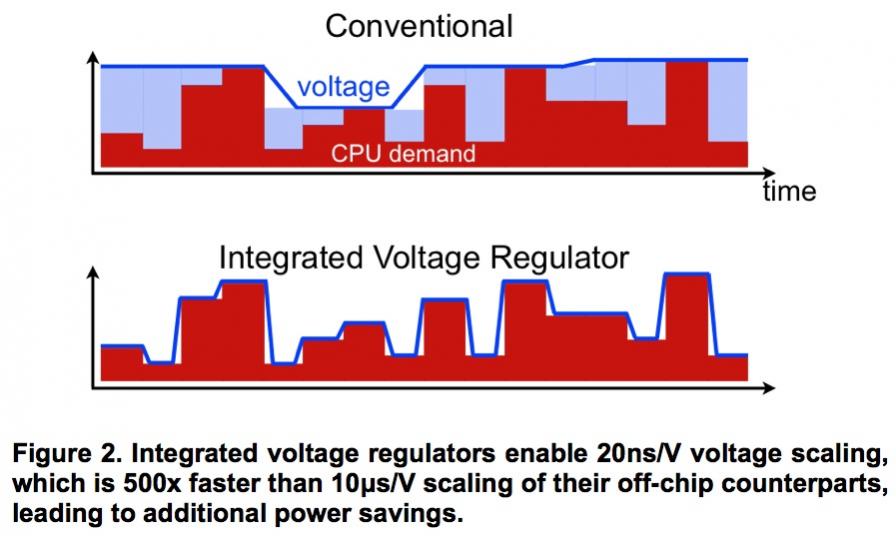
2) DVFS: slow voltage scaling time. (Figure 2)
3) Power Gating: slow to turn on from off-state, lose data when powered off
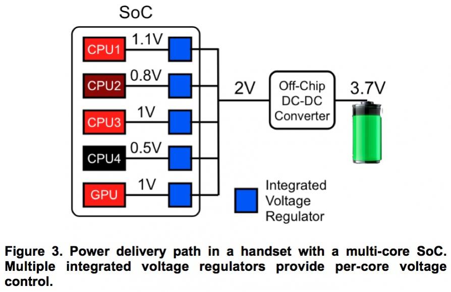
One way to enable per-core voltage control is to use multiple off-chip switching DC-DC converters, but the bulk of off-chip components make this solution expensive. Instead, we propose to design voltage regulators small enough to integrate on the same die as the SoC. Multiple integrated voltage regulators (IVR) can be duplicated for per-core voltage control (Figure 3). IVRs offer 20ns/V voltage scaling time, which is 500x faster than the 10μs/V of conventional off-chip DC-DC converters, enabling fast, per-core DVFS. This allows the SoC to reduce the voltage during relatively short time periods, i.e. ~200 cycles while waiting for a L2 cache miss to return, or boost the voltage to speedup the execution of critical sections.

To maximize the benefits of IVRs, it is critical to minimize conversion loss and on-die area overhead while providing a wide range of output voltage for DVFS. Linear regulators incur larger conversion loss as output voltage is reduced for DVFS. Widely used buck converters (inductor-based) require large inductors, which is especially problematic for on-die integration. We present a 3-level IVR that enables a smaller on-chip spiral inductor (1nH) compared to a buck converter [ISSCC ’11].
SoCs can integrate IVRs as IP blocks attached to each core. This solution provides tight voltage control, but adds <5% die area on SoCs implemented in cutting edge technologies, potentially increasing cost. An alternative is to implement IVRs on a separate chip using a cheaper and older technology and have a package contain both the processor and IVR die. Intel presented a system-in-package containing a buck converter die implemented in 130nm technology and a Core2Duo processor [APEC ’10]. This technology can also be used to design power management IC (PMIC) chips with smaller and fewer off-chip components.
In conclusion, IVRs have the potential to 1) reduce power of multi-core SoCs, 2) reduce the number and thickness of board components 3) enable lighter, thinner portable electronics. IVRs can be used in high-performance processors and FPGAs as well as low-power SoCs.

References:
A Fully-Integrated 3-Level DC/DC Converter for Nanosecond-Scale DVS with Fast Shunt Regulation
Wonyoung Kim, David Brooks, Gu-Yeon Wei
IEEE International Solid-State Circuits Conference (ISSCC), 2011.
A 60MHz 50W Fine-Grain Package-Integrated VR Powering a CPU from 3.3V
Gerhard Schrom, Fabrice Paillet, Jaehong Hahn
IEEE Applied Power Electronics Conference (APEC), 2010.


Solving the EDA tool fragmentation crisis