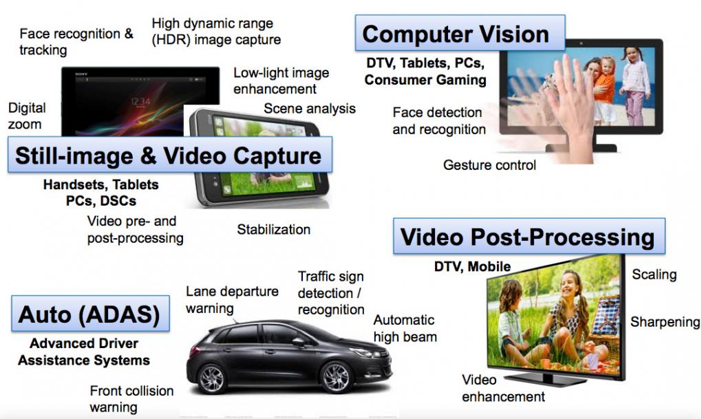
 Video is a huge growing area and advanced imaging applications are becoming ubiquitous. By “advanced” I mean more than just things like cameras in your smartphone. There is lots more coming, from high-dynamic range (HDR) photography, gesture recognition, more and more intelligent video in cars to keep us safe, face-recognition and so on. And not at the resolutions that we are used to, things are going ultra-high definition (UHD) with 4Kx2K pixels, 18 megapixel cameras (in our phones). Result, video processing requirements are doubling every 18 months whereas Moore’s law is doubling more like every 3 years these days.
So what’s a designer to do? The application processor chip in a smartphone already has some cores, can’t we use them? It probably had a dual/quad core ARM Cortex of some sort. It probably has a dual or quad core GPU, maybe from Imagination. It probably already has some specialized video circuitry such as H.264 encode and decode. Isn’t that enough? Even ignoring power this is not enough processing performance for many of these new applications. With a realistic power limit it is not even close. Video didn’t just kill the radio-star, it is killing the power budget too.
First the ARM. High-resolution video processing requires at least 4 cores but at 1.5GHz that is 3W, which is about 10 times the power budget. But at least it is easy to program. If we try and use the GPU for the image processing, it is not a very good match since the GPU is focused on floating point and 3D graphics. Plus GPUs are notoriously hard to program for anything other than the graphics pipeline for games etc. Using dedicated hardware can work well for anything like codecs where the standards are fixed (for a decade or so) but the new application areas are in flux with the algorithms changing all the time. And while adding a couple of specialized blocks can be attractive compared to using that ARM, the tradeoff doesn’t look so good once you get up to a dozen or more blocks. They take up a lot of area and consume a lot of power.

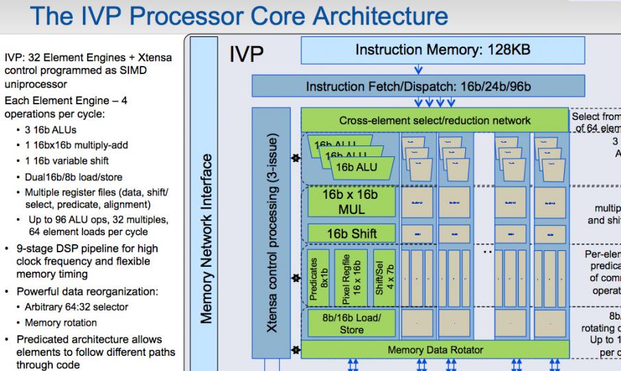
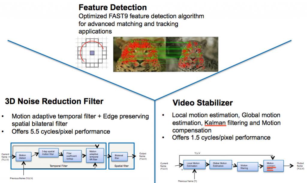
Today Tensilica is announcing their Imaging Video Processor (IVP) family and the first member of the family. Of course under the hood this is built on top of the Xtensa VLIW processor generation technology and the associated software technology (vectorizing compilers, modeling etc) that go with it. So while the video aspects are new the fundamental technology is mature.
Of course the focus is on low-power handheld devices since these have the most severe constraints: low power budgets, consumer price points and product cycles. The IVP hits the sweet spot between ease of programming and energy efficiency.

The core is licensable but that’s not all there is. RTL, EDA scripts, Instruction-set simulator, IDE (Eclipse-based), C compiler, debugger, image processing applications, operating systems, documentation. And software partners with deep video expertise who work on the bleeding edge of video algorithms.
In the crucial measure of 16b pixel operations per second per watt, IVP is about 10 to 20X as efficient as using the ARM Cortex, and about 3 to 6X as efficient as using the GPU. All with the programming flexibility of a software implementation, a big advantage over direct implementation in RTL in an area where tweaks to algorithms and even entirely new algorithms are commonplace.
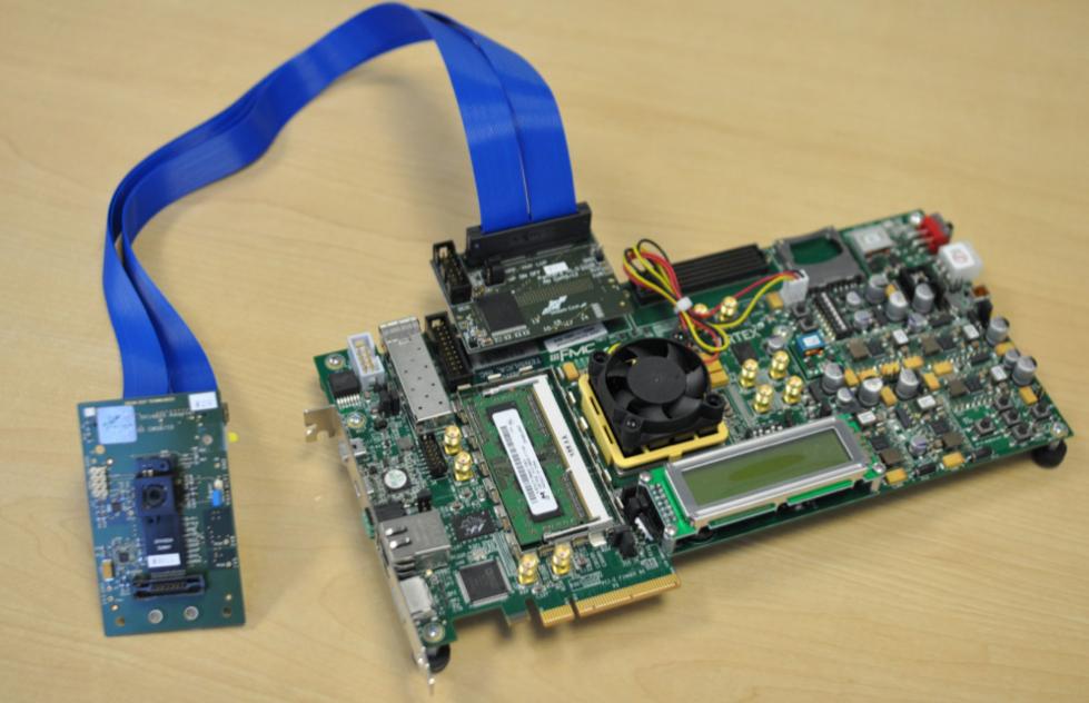
 Oh, and there is an FPGA development platform too, so that you can hook up an IVP to cameras, TVs, screens or whatever.
Tensilica will be showing the new product in Barcelona at Mobile World Congress at the end of the month. They are in Hall 6 at booth D101. If you are lucky enough to be in Barcelona, one of my favorite European cities, then go by and see them. And don’t miss all the amazing Gaudi architecture. Or the Miro museum. And tapas on la Rambla.
More details on Tensilica’s website here.


Intel, Musk, and the Tweet That Launched a 1000 Ships on a Becalmed Sea