 In the embedded world that drives much of today’s ASIC innovation, there is no bigger name than ARM. Not to enter the ARM vs. Intel fray, but it’s no exaggeration to say that ARM’s impact on SoCs is as great as Intel’s on the PC. Few cutting edge SoCs are coming to market that do not include some sort of embedded processor. And a disproportionately large number of those processors are from ARM.
It stands to reason then, that the capability to design and implement ARM into ASIC SoCs is paramount and so I used some of my time at DAC to check out what was happening in the ARM design and implementation space. To that end, I was very pleased with what I found at the GUC demonstration.
For those few of you who may not know, GUC, orGlobal Unichip Corp., is leading the charge into a new space called the Flexible ASIC Model[SUP]TM[/SUP]. The Flexible ASIC Model, according to GUC, allows semiconductor designers to focus on their core competency while providing a flexible handoff point for each company, depending on where their core competency begins and ends. The model accesses foundry design environments to reduce design cycle time, provides IP, platforms and design methodologies to lower entry barriers, and integrates technology availability (design, foundry, assembly, test) for faster time–to–market. In a nutshell, the company should have a great deal of insight into how to integrate ARM based processors into ASIC innovation.
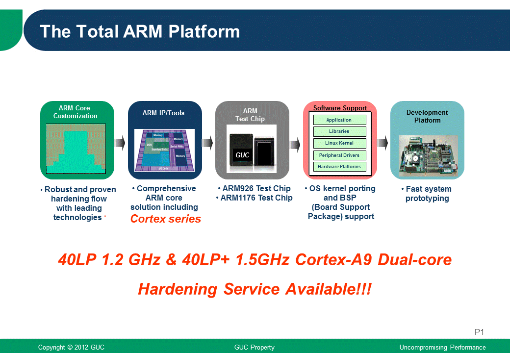
Not surprisingly, GUC has dedicated significant resources to successfully embedding ARM processors into ASIC designs. The service covers a robust and proven hardening flow that targets leading edge manufacturing process technologies, ARM-specific IP and design, successful test chips for ARM926, ARM1176 and the Cortex series, software support and a development platform that includes fast system prototyping.

The ARM hardening process starts with RTL validation that includes specification confirmation and memory integration. The next step, synthesis, covers critical path optimization and timing constraint polishing. Design for test (DFT) includes MBIST integration, scan insertion and compression, at-speed DFT feature integration and test coverage tuning. Place and route services cover floor planning and placement refinement, timing closure, dynamic and leakage power analysis, IR/EM analysis, dynamic IR analysis, design for manufacturing (DFM), and DRC/LVS. Final quality assurance (QA) covers library consistency review, log parsing, report review and checklist item review.
GUC’s ARM core hardening service also includes document deliverables including application nodes and simulation report. Normally, after receiving customers’ specification requests, GUC provides a preliminary timing model within one month and completes the design kit within two months.
Most importantly, their methodology has been proven. GUC recently broke the one Gigahertz barrier with an ARM Cortex-A9 processor and their history with ARM stretches back over a decade. During that time, the company has successfully run more than 90 ARM core tape outs with proven production at high yields for different applications (high performance, low power) on multiple TSMC process nodes (28nm, 40nm, 65nm, 90nm).
The importance that ARM cores will play as ASIC SoC innovation moves forward is still largely untold. But what is clear is that an ARM hardening process will be required for ASIC success. Given the complexity, this may be a difficult service to move in-house and so finding ASIC companies with critical, proven ARM hardening capabilities will become an increasingly important ingredient in the success formula.


Musk’s Orbital Compute Vision: TERAFAB and the End of the Terrestrial Data Center