You are currently viewing SemiWiki as a guest which gives you limited access to the site. To view blog comments and experience other SemiWiki features you must be a registered member. Registration is fast, simple, and absolutely free so please,
join our community today!
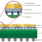
A couple of weeks ago, Xilinx and TSMC announced the production release of the Virtex-7 HT family, the industry’s first heterogeneous 3D ICs in production. With this milestone, all Xilinx 28nm 3D IC families are now in volume production. These 28nm devices were developed on TSMC’s Chip-on-Wafer-on-Substrate (CoWoS)… Read More
It is important to note that the System On Chip (SoC) revolution that is currently driving mobile electronics has one very important enabling technology and that is Semiconductor Intellectual Property. Where would we be without the commercial IP market segment? Computers and phones would still be on our desks for one thing, and… Read More
Kevin Ashton, a British technology pioneer, is credited for the term “The Internet of Things” to describe an ecosystem where the Internet is connected to the physical world via ubiquitous sensors. Simply stated: rather than humans creating content for the internet IoT devices create the content. To be clear, this… Read More
As semiconductors become more integrated into our lives reliability is becoming a critical issue. As IP consumes more of our die, IP reliability is becoming a critical issue. As we pack more transistors into a chip, reliability is becoming a critical issue. As we move from 28nm to 20nm to 16nm, reliability is becoming a critical … Read More
Taiwan Semiconductor Manufacturing Corporation is the world’s leading semiconductor foundry by revenue and, by extension, profitability. While I am deeply saddened that current CEO Morris Chang will be retiring (again) shortly, I am hopeful that his successor will be able to continue the legacy of foundry industry leadership… Read More
Success in manufacturing has two conditions: tariff barriers to shield the infant industries from external competition, and a rigorous focus on exports to ensure that manufacturing cannot just shelter behind the tariff barriers and reap monopoly profits inside the country. Each industry needs to have several companies enter,… Read More
Analog and mixed-signal ICs are tougher to design and verify compared to digital, so if you want to learn more about best practices from actual AMS engineers then consider attending a summitthat is sponsored by Cadence Design Systems next Thursday, October 10th in San Jose from 8:00AM until 6:30PM.
They’ve lined up an interesting… Read More
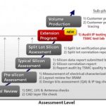
One of the highlights of the TSMC 2013 Open Innovation Platform® Forum was the Partner Award Ceremony. TSMC awarded Berkeley Design Automation (BDA) with the TSMC Open Innovation Platform’s Partner of the Year Award 2013 for joint development of 16nm FinFET design infrastructure. I talked with Ravi Subramanian, BDA CEO,… Read More
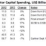
Global semiconductor capital spending is headed for another decline in 2013, following a 12% decline in 2012. Gartner’s September forecast called for a 7% decline in 2013. Most of the major spenders expect flat to declining expenditures in 2013. Intel in July estimated 2013 spending of $11 billion, flat with 2012 and down from … Read More
The legend of Intel being two process nodes ahead of the rest of the industry is quickly coming to an end. To come to terms with this you need to do an apple to apple comparison which is what I will do right here, right now.
First and foremost let’s compare SoC silicon delivery since SoCs are driving the semiconductor industry and will … Read More