In 1992, when Samsungbecame the largest producer of memory chips, it was not in top10 list of semiconductor companies. It was ranked at #11. Since then it has strived to attain higher ranks in the top10 list. In around 2000, it climbed to the ranks of top5 and then since 2002 until now it is at #2 in the worldwide semiconductor sales which… Read More

Tag: tsmc
IP Market at Your Desk!
Semiconductors have played very important role in making internet successful and that has unleashed the potential of e-commerce. Today, we see names like Alibaba, whose primary focus is on commodity trade. I couldn’t imagine an e-commerce type of web portal for semiconductor services until I looked at the eSilicon website. … Read More
Altera Back to TSMC at 10nm? Xilinx Staying There
Xilinx announced their quarterly results last week. They slightly missed their number due mainly to a decline in wireless sales. Of course Xilinx parts don’t go in the smartphones since the cost and power are too high, but they are very heavily used in basestation, backhaul etc especially in China. Xilinx’s business… Read More
Will the Apple A9 Fall Flat?
Several months ago we had suggested that we were concerned that Apple’s A9 processor would wind up being 20nm planar (maybe 14nm planar) rather than the expected 14nm FinFET. As we are now under 9 months from a likely launch time for Apple’s next gen IPhone the timing for getting a 14nm FinFET processor on board the phone… Read More
Apples Versus Zebras
I have seen a couple of posts comparing the density of the Apple A8 to the Intel Core M and concluding that the TSMC 20nm process is denser than the Intel 14nm process. In one of the threads one of the posters likened this to comparing apples to oranges, I agree except I think it is even worse than that, I think it is more like comparing apples… Read More
IEDM Advanced CMOS Technology Platform Session
First I want recognize that IEDM once again provided all of the attendees with the proceedings as soon as we arrived at the conference, in fact the proceeding included every year of IEDM back to 1955. This is how a conference should be run! Anyone who read my blog about the SPIE Advanced Lithography Conference will know how frustrating… Read More
ANSYS Updates RedHawk for FinFET Nodes
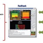
Most designers are not using FinFETs yet, however the increased transistor density and power advantages they offer are compelling. Smaller feature sizes have been a consistent driver in semiconductor technology. Eventually the market will move more and more to FinFET processes, increasingly leaving behind planar transistors.… Read More
Is Fab Business The Forte of APAC?
A little ago, I was looking at the top20 semiconductor companies in the world and was surprised to see a couple of large companies in Taiwan and South Korea garnering >34% of total sales (See – Look who is Leading the World Semiconductor Business). This time it’s another surprise, when I look at IC Insights report on global 300mm… Read More
Results of TSMC’s ECO Fill Flow
By Jeff Wilson, Mentor Graphics and Anderson Chiu, TSMC
At this year’s TSMC Open Innovation Platform® (OIP) Ecosystem Forum, Mentor Graphics and TSMC co-presented some results of the ECO Fill flow developed for TSMC customers working at advanced nodes. Here is a summary of the presentation. (TSMC customers can access the presentation… Read More
IEDM: TSMC, Intel and IBM 14/16nm Processes
This week is IEDM. Three of the presentations today were by TSMC, Intel and IBM going over some of the details of their 14/16nm processes. They don’t provide the slides at IEDM, just the single page papers so this may end up being a somewhat random collection of facts.
TSMC were up first. They talked about the improvements that… Read More