You are currently viewing SemiWiki as a guest which gives you limited access to the site. To view blog comments and experience other SemiWiki features you must be a registered member. Registration is fast, simple, and absolutely free so please,
join our community today!
During SNUG I took the opportunity to chat to Choon-Hoe Yeoh of Lattice Semiconductor about how they use Concept Engineering’s Starvision Pro product. He is the senior director of EDA tools and methodologies there.
Lattice Semiconductor is a manufacturer of low-power, small-footprint, low-cost programmable logic devices.… Read More
It has been about a year since the acquisition of Berkeley Design Automation by Mentor Graphics. Berkeley was doing quite well in the somewhat crowded SPICE simulator market. In many respects they broke new ground for high speed and accurate SPICE simulators. Since the acquisition we know that former Berkeley executives are now… Read More
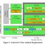
Power regimes for contemporary SOC’s now include a large number of voltage domains. Rail voltages are matched closely to the performance and power requirements of various portions of the design. Indeed, some of the supply voltages are so low that the noise margins in these domains is exceedingly low. Higher voltage domains are… Read More
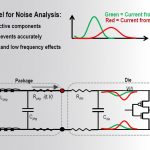
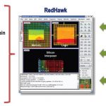
Often substrate noise analysis takes place when everything is there on the chip, but that stage comes near the tape-out which is too late to make major changes in architecture, placement, introducing noise protection circuitry for the victims and so on. It was okay when there used to be very little analog content on the chip. But … Read More
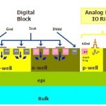
These days it’s common to expect large digital designs, analog blocks, custom IPs, glue logic, interfaces and interconnects all developed separately, perhaps by different vendors / teams, but integrated together in a single environment forming an SoC. The SoC can have multiple clock domains and can work in multiple modes of … Read More
I had been wanting to write about it since Google’sbig bang announcement of Android1 in India in Sep this year and their associated strategy to capture some of the large pockets of Smartphone market within a matured or declining cell phone market and maturing overall market of Smartphone. Since I wrote my last article hereon maturation… Read More
I think by now there has been good level of discussion on FinFET technology at sub-20 nm process nodes and this is an answer to ultra dense, high performance, low power, and billion+ gate SoC designs within the same area. However, it comes with some of the key challenges with respect to power, noise and reliability of the design. A FinFET… Read More
The success of our semiconductor eco-system depends on collaboration, so the annual TSMC OIP Event just held on September 30 at the San Jose Convention Center was a prime example of that. I didn’t attend this year, but I did follow up with Amit Nandaof Silvaco this week to hear about what they presented. As a consultant I’ve… Read More
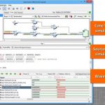
In today’s SoC world where multiple analog and digital blocks along with IPs at different levels of abstractions are placed together on a single chip, debugging at all levels becomes quite difficult and clumsy. While one is working at the top level and needs to investigate a particular connection at an intermediate hierarchical… Read More
SiC and Si Power Devicesby Daniel Payne on 09-27-2014 at 7:00 amCategories: EDA
ICs for consumer electronics are often battery powered, which are considered low voltage designs. On the other end of the IC spectrum are high voltage devices used in many industrial applications like: automotive, aerospace, data centers, transportation and power generation. … Read More