You are currently viewing SemiWiki as a guest which gives you limited access to the site. To view blog comments and experience other SemiWiki features you must be a registered member. Registration is fast, simple, and absolutely free so please,
join our community today!
At the GSA silicon summit yesterday the first keynote was by Subramanian Iyer of IBM on Keeping Moore’s Law Alive. He started off by asking the question “Is Moore’s Law in trouble?” and answered with an equivocal “maybe.”
Like some of the other speakers during the day, he pointed out that … Read More
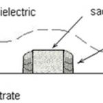
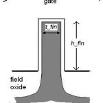
The previous post in this series provided an overview of FinFET devices. This article will briefly cover FinFET fabrication.
The major process steps in fabricating silicon fins are shown in Figures 1 through 3. The step that defines the fin thickness uses Sidewall Image Transfer (SIT). Low-pressure chemical vapor (isotropic)… Read More
If you are in Europe then the CDNLive! EMEA user conference is in Munich at the Dolce Hotel from May 14th to 16th. Like last month’s CDNLive! in Cadence’s hometown San Jose, the conference focuses on sharing fresh ideas and best practices for all aspects of semiconductor design from embedded software down to bare silicon.… Read More
Do you need more servers? Do you need more licenses? If you are kicking off a verification run of 10,000 jobs on 1,000 server cores then you are short of 9000 cores and 9000 licenses, but you’d be insane to rush out with a purchase order just on that basis. Maybe verification isn’t even on the critical path for your design,… Read More
For a long time Cisco had a very high end product whose official internal name during its years of development was HFR, which stood for Huge F***ing Router (the marketing department insisted it stood for ‘fast’). Eventually it got given a product number, CRS-1, but not before I’d read an article about it in the… Read More
With the recent closure of the Synopsys Magma deal and the economy showing a bit of uptick and some positive outlook compared to the last 3-4 years, I believe it’s time for some of the creative minds that find themselves looking for new opportunity to consider starting their own point tool as well as IP companies.
Many of these people… Read More
Who doesn’t love the perennial Hogan’s Heros panel at DAC? Always provocative and illuminating, for technologists, entrepreneurs, and strategists.
At DAC 2012, Jim Hogan’s panel is “Learning from Apple”:Apple. We admire their devices, worship their creators and praisetheir stock in our portfolios. Apple is synonymous with… Read More
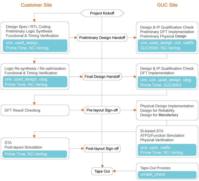
During my last Taiwan trip I also spent time with Global Unichip. Clearly, in order for the semiconductor industry to thrive we must enable design starts. With the rising costs and complexity of semiconductor design and manufacturing this is a much greater challenge which is why I’m so interested in GUC, for the greater good of the… Read More
The Carbon Decadeby Paul McLellan on 04-19-2012 at 6:00 amCategories: Arm, EDA, IP
Carbon Design Systems celebrates its 10th anniversary this month. It is a celebration that the company has survived a decade but also bittersweet that the company hasn’t been acquired for a juicy premium. But we just have to accept that EDA is not a business where you can throw together a company in 18 months and sell it for $1B… Read More
This is the first of a multi-part series, to introduce FinFET technology to SemiWiki readers. These articles will highlight the technology’s key characteristics, and describe some of the advantages, disadvantages, and challenges associated with this transition. Topics in this series will include FinFET fabrication,… Read More