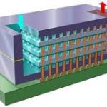
A three-dimensional integrated circuit (3D IC ) is a chip in which two or more layers of active electronic components are integrated both vertically and horizontally into a single circuit. The semiconductor industry is hotly pursuing this emerging technology in many different forms, as a result the full definition is still somewhat… Read More
Tag: semiconductor
Analyzing and Planning Electro-static Discharge (ESD) Protection
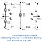
ESD has historically been a big problem analyzed with ad-hoc approaches. As explained earlier, this is no longer an adequate way to plan nor signoff ESD protection.
Pathfinder is the first full-chip comprehensive ESD planning and verification solution. It is targeted to address limitations in today’s methodologies.… Read More
FPGA Prototypes Made Easy
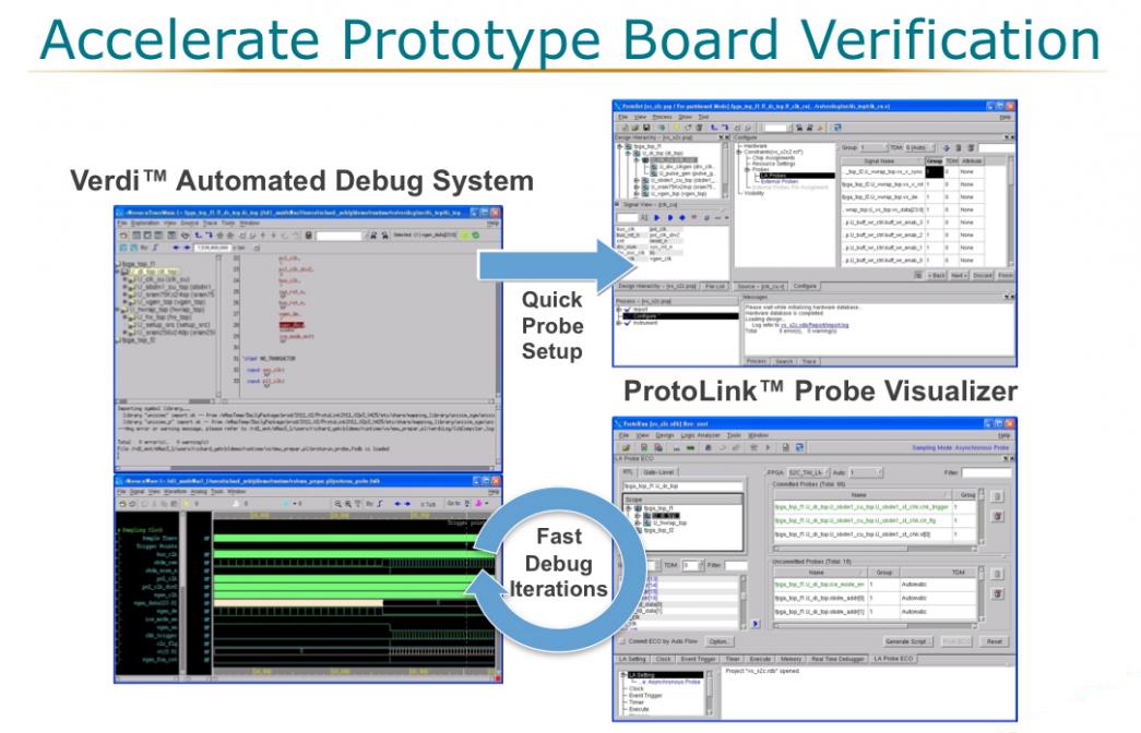
FPGA-based prototype boards are a fast, cost-effective platform for SoC system validation but they are notoriously difficult to set up and to debug. There is a big upside, however, allowing early software integration and testing and thus finding bugs in both the software and the SoC earlier. This approach is much cheaper than … Read More
Adjusting Custom IP to Process Changes
A High-Definition Multimedia Interface (HDMI) IP core was being implemented in an advanced process technology. This fairly large and complex analog mixed-signal (AMS) IP comprising over 130K devices was close to being finalized and shipped to the customer. But many design rules at the foundry were unexpectedly changed from… Read More
SOC Realization: How Chips Are Really Designed
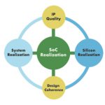
If you just casually peruse most marketing presentations by EDA companies, you’d come to the conclusion most SoCs are designed from scratch, wrestlilng the monster to the ground with bare hands. But the reality is that most SoCs consist of perhaps 90% IP blocks (many of them memories). That still leaves the remaining 10% … Read More
40nm to 28nm Migration Success Story
The problem:To move dual-port SRAM library and macros from a 40nm process to a 28nm process. In addition to all the changes between two different foundry processes, the 28nm rules are disruptive and incompatible with the previous rules. The memory corecells (foundry-specific) would also need to be completely replaced.
Current… Read More
Chip Power Models
As the complexity of the chip-package-system (CPS) interactions has increased, the tradeoffs in doing a power and noise analysis has had to gradually increase. As is so often the case in semiconductor designs, issues first arise as second-order effects that can largely be ignored but each process node makes the problem worse … Read More
Mentor 2 : Carl Icahn 0
The corporate raiders are still throwing rocks at Mentor Graphics. I have followed this reality show VERY closely and find their latest assault seriously counterproductive. Disinformation is common in EDA but I expected more from Carl Icahn and the Raiderettes. They are quite the drama queens. Here is a billion dollar question:… Read More
Ivo Bolsens of Xilinx and Crossover Designs
I was at Mentor’s u2u (user group) meeting and one of the keynotes was by Ivo Bolsens of Xilinx. The other was by Wally Rhines and is summarized here.
Ivo started off talking analogizing SoCs as the sports-cars of the industry (fast but expensive), and FPGAs as the station wagons (not cool). In fact he even said that when Xilinx… Read More
Wally’s u2u keynote
I was at Wally’s u2u (Mentor user group) keynote yesterday. The other keynote was by Ivo Bolsens of Xilinx and is here. He started off by looking at how the semiconductor industry has recovered and silicon area shipments are now back on trend after a pronounced drop in 2009 and revenue has followed. Finally the semiconductor… Read More


