You are currently viewing SemiWiki as a guest which gives you limited access to the site. To view blog comments and experience other SemiWiki features you must be a registered member. Registration is fast, simple, and absolutely free so please,
join our community today!
The 63rd annual IEDM (International Electron Devices Meeting) will be held December 2nd through 6th in San Francisco. In my opinion IEDM is one of, if not the premier conference on leading edge semiconductor technology. I will be attending the conference again this year and providing coverage for SemiWiki. As a member of the press… Read More
At the imec technology forum held at SEMICON West, Martin Van Den Brink, President and CTO of ASML presented on the latest developments on EUV. I also had an opportunity to sit down with Mike Lercel, ASML Director of Strategic Marketing for an interview.… Read More
I have previously published analysis’ converting leading edge logic processes to “standard nodes” and comparing standard nodes by company and time. Recently updated details on the 7nm process node have become available and in this article, I will revisit the standard node calculations and trends.… Read More
For many year 2D NAND drove lithography for the semiconductor industry with the smallest printed dimensions and yearly shrinks. As 2D NAND shrunk down to the mid-teens nodes, 16nm, 15nm and even 14nm, the cells became so small that there were only a few electrons in each cell and cross-talk issues made further shrinks very difficult… Read More
At the SPIE Advanced Lithography Conference imec published a number of papers on EUV, multi-patterning and other lithography issues. In addition to seeing several of the papers presented I had a chance to sit down with imec’s director of advanced patterning, Greg McIntyre. In this article I will summarize my discussions… Read More
As feature sizes have shrunk, the semiconductor industry has moved from simple, single-exposure lithography solutions to increasingly complex resolution-enhancement techniques and multi-patterning. Where the design on a mask once matched the image that would be produced on the wafer, today the mask and resulting image … Read More
Irresistible Materials (IM) is a spin-out of the University of Birmingham in the United Kingdom that has been doing research on Photoresist and Spin-On Carbon hard masks for 10 years, most recently with Nano-C on chemistry development. IM has developed a unique EUV photoresist and they are now looking for partners to help bring… Read More
Yesterday I attended Intel’s manufacturing day. This was the first manufacturing day Intel has held in three years and according to Intel their most in depth ever.
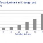
Nodes must die
I have written several articles comparing process technologies across the leading-edge logic producers – GLOBALFOUNDRIES, Intel, Samsung… Read More
The annual SPIE Advanced Lithography Conference kicked off last night with vendor sponsored networking events and such. SPIE is the international society for optics and photonics but this year SPIE Advanced Lithography is all about the highly anticipated EUV technology. Scotten Jones and I are at SPIE so expect more detailed… Read More
SPIE is the premier event for lithography held in Silicon Valley and again Scotten Jones and I will be attending. EUV is generally the star of the show and this year will be no different now that TSMC has committed to EUV production in 2019.
Last year at SPIE, TSMC presented the history of EUV development from the beginning in 1985 as … Read More