You are currently viewing SemiWiki as a guest which gives you limited access to the site. To view blog comments and experience other SemiWiki features you must be a registered member. Registration is fast, simple, and absolutely free so please,
join our community today!
It has been an exciting time in the semiconductor industry and the excitement is far from over. Years 2022 and 2023 will be more challenging in many different ways and live activities have just begun. The cornerstones to the semiconductor industry are the foundries so I look forward to the live foundry events coming up in October,… Read More
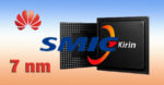
Recently TechInsights analyzed a Bitcoin Miner chip fabbed at SMIC and declared SMIC has a 7nm process. There has been some debate as to whether the SMIC process is really 7nm and what it means if it is 7nm. I wanted to discuss the case for and against the process being 7nm, and what I think it means.
First off, I want to say I am not going … Read More
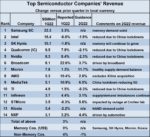
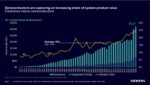
The semiconductor market in 2022 is weakening. Driving factors include rising inflation, the Russian war on Ukraine, COVID-19 related shutdowns in China, and lingering supply chain issues. Four of the top 14 semiconductor companies (Intel, Qualcomm, Nvidia and Texas Instruments) are expecting lower revenues in 2Q 2022 versus… Read More
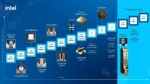
As I previously wrote about here, Intel is presenting their Intel 4 process at the VLSI Technology conference. Last Wednesday Bernhard Sell (Ben) from Intel gave the press a briefing on the process and provided us with early access to the paper (embargoed until Sunday 6/12).
“Intel 4 CMOS Technology Featuring Advanced FinFET Transistors… Read More
One of the recent live events I attended was the 2022 GSA Silicon Leadership Summit on May 12th at the Santa Clara Convention Center (my favorite location). This was the first GSA live event in two years so it was a must attend gathering. This event targets semiconductor ecosystem executives (200+ people attended) so there were many… Read More
The VLSI Symposium on Technology & Circuits will be held in Hawaii from June 12th to June 17th. You can register for the conference here.
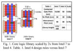
The tip sheet for the conference has been released and one thing that caught my eye is some data from the Intel 4 paper that Intel will be presenting at the conference.
Intel’s old roadmap had 14nm,… Read More
Earlier this year semiconductor oracle Malcom Penn did his 2022 forecast which I covered here: Are We Headed for a Semiconductor Crash? The big difference with this update is the black economic clouds that are looming which may again highlight Malcolm’s forecasting prowess. I spent an hour with Malcolm and company on his Zoom cast… Read More
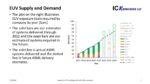
In my “The EUV Divide and Intel Foundry Services” article available here, I discussed the looming EUV shortage. Two days ago, Intel announced their first EUV tool installed at their new Fab 34 in Ireland is a tool they moved from Oregon. This is another indication of the scarcity of EUV tools.
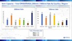
I have been tracking EUV system production… Read More
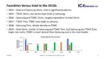
At the ISS conference held from April 4th through 6th I presented on who I thought would have the leading logic technology in 2025. The following is a write up of that presentation.
ISS was a virtual conference in 2021 and I presented on who currently had logic leadership and declared TSMC the clear leader. Following that conference,… Read More
The EUV Divide
I was recently updating an analysis I did last year that looked at EUV system supply and demand, while doing this I started thinking about Intel and their Fab portfolio.
If you look at Intel’s history as a microprocessor manufacturer, they are typically ramping up their newest process node (n), in volume production… Read More