You are currently viewing SemiWiki as a guest which gives you limited access to the site. To view blog comments and experience other SemiWiki features you must be a registered member. Registration is fast, simple, and absolutely free so please,
join our community today!
When most people hear the term PDF, they immediately think of a PDF file, a universal, platform-independent way to share electronic documents.
There is, however, another PDF that many outside the semiconductor industry may not be familiar with. And this PDF actually predates the PDF file format. It is short for PDF Solutions, … Read More
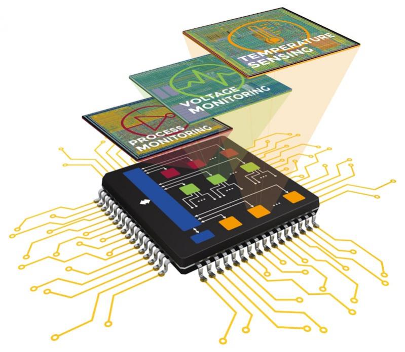
In an era defined by complex chip architectures, ever-shrinking technology nodes and very demanding applications, Silicon Lifecycle Management (SLM) has become a foundational strategy for optimizing performance, reliability, and efficiency across the lifespan of a semiconductor device. Central to effective SLM are Process,… Read More
The annual International Electron Devices Meeting (IEDM) took place last month. One of the presentations on the short course was by Matthew Metz of Intel titled New Materials Systems for Moore’s Law Continuation. In essence this was a look at some of the possibilities for what comes after silicon runs out of steam.
Matthew started… Read More
I used to be part of the custom silicon management team at Apple. I’ve seen how great a challenge it is to pull off a custom silicon strategy within a one year product cycle. Apple is the perfect example of this custom silicon model since they develop the best mobile processors in the world for their products. Which also includes other… Read More
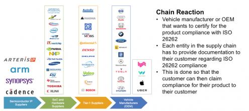
Everyone up and down the electronics supply chain is jumping on the ISO 26262 bandwagon and naturally they all want to show that whatever they sell is compliant or ready for compliance. We probably all know the basics here – a product certification from one of the assessment organizations, a designated safety manager and a few other… Read More
In the old days to learn about new semiconductor IP you would have to schedule a sales call, listen to the pitch, then decide if the IP was promising or not. Today we have webinars which offer a lot less drama than a sales call, plus you get to ask your questions by typing away at the comfort of your desk, hopefully wearing headphones as … Read More
When working on an analog design, after initial design specs have been met, it is useful to determine if the design meets specs out to 3 or 4 sigma based on process variation. This can serve as a useful step before going any further. It might not be a coincidence that foundries base their Cpk on 3-sigma. To refresh, Cpk is the ratio of the… Read More
Product lifecycle management is probably not the most gripping topic for most design engineers. You want to get on with architecture, design, verification and implementation. But if you are building products for any safety-sensitive application in a car, a medical appliance, avionics, railway applications in Europe – to name… Read More
The design community is always hungry for high-performance, low-power, and low-cost devices. There is emergence of FinFET and FDSOI technologies at ultra-low process nodes to provide high-performance and low-power requirements at lower die-size. However, these advanced process nodes are prone to new sources of variation.… Read More
Not only are foundries continuing to introduce processes at new advanced nodes, they are frequently updating or adding processes at existing nodes. There are many examples that illustrate this well. TSMC now has 16FF, 16FF+ and now 16FFC. They are also announcing 10nm and 7nm processes. In addition, they are going back to older… Read More


