You are currently viewing SemiWiki as a guest which gives you limited access to the site. To view blog comments and experience other SemiWiki features you must be a registered member. Registration is fast, simple, and absolutely free so please,
join our community today!
Semiconductor design automation at system level is gaining its due importance today. It needs an effective, efficient, and seamless flow from system up to silicon. There is lot of effort going on for automating SoC design exploration at system level but that eventually stops at RTL; another level of flow automation takes over … Read More
Only one company at the recent DAC conference and exhibit had a set of four interacting disciplines: Fluids, Structures, Electronics and Systems. Did you guess that the company was ANSYS? I get so IC focused at times that I almost forget that chips plug into boards, that boards become systems, and that systems drive and control mechanical… Read More
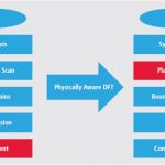
Introducing on-chip test circuitry has become a necessary criteria for an ASIC’s post manufacture testability. The test circuitry is usually referred as DFT (Design-for-Test) circuit. A typical methodology for introducing DFT circuit in a design is to replace usual flip-flops with special types of flip-flops called ‘scan… Read More
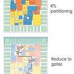
Complex SoC project teams typically use a divide and conquer approach where specialized engineers work in separate domains, like front-end or back-end. The five major engineering tasks for IC design can be described as: RTL design, synthesis, floor planning, place and route, then finally design analysis.
What if you could detect… Read More
If we look at the past, most of the EDA tools in the semiconductor design space have originated from a designers’ need to do things faster. Regardless of whether it is design exploration, manual design, simulation, verification, optimization (Power Performance Area – PPA) and many other steps in the overall design flow.… Read More