You are currently viewing SemiWiki as a guest which gives you limited access to the site. To view blog comments and experience other SemiWiki features you must be a registered member. Registration is fast, simple, and absolutely free so please,
join our community today!
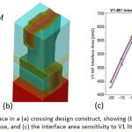
The traditional system-on-chip (SoC) design process has fully qualified verification methods embodied in the form of process design kits (PDKs). Why is it that chip design companies and assembly houses have no IC/package co-design sign-off verification process?
Package die are often produced using multiple processes and… Read More
Earlier in the week I wrote about GlobalFoundries announcement of 22nm FD-SOI. At SEMICON West there were three events that filled in some more details. First, on Tuesday, a lunch presentation given by SOITEC who make the wafer blanks that FD-SOI requires. Then on Wednesday I sat down for an hour with Gary Patton and Subi Kengeri … Read More
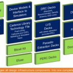
For any semiconductor technology node to be adopted in actual semiconductor designs, the very first step is to have a Process Design Kit (PDK) developed for that particular technology node and qualified through several design tools used in the design flow. The development of PDK has not been easy; it’s a tedious, time consuming,… Read More
The simple answer is when everything in the world is smart. But if you think deeply, you would find that the continuous progression to make things easy in life is what makes the world smarter day-by-day – the sky is the limit. In the world of computing, consider the 17[SUP]th[/SUP] century era when humanbrain was used as a computer … Read More
In the semiconductor ecosystem, several partners (or better to say stakeholders) join together in the overall value chain to finally output the most coveted chip, err I should say SoC these days. It becomes really interesting when we start analyzing the real value added by each of them, none appears to be less. Well, then to whom … Read More
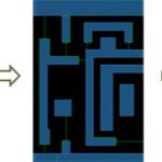
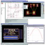
Exactly a year ago Sage Design Automation launched its revolutionary iDRM product, enabling for the first time to graphically capture design rules and compile them into checks automatically – no programming required. Using the graphical design rule editor, users could draw the layout topology that describes the design… Read More
Ever since I started talking about Virtual Fabrication I have mostly looked at it from the manufacturers’ perspective, where it has obvious benefits to develop and model new process technology. But what about the fabless design concept and indeed even the semiconductor IP world that has spawned from it as well? It seems that Virtual… Read More
TowerJazz and Silvaco BFFby admin on 11-15-2013 at 1:04 pmCategories: EDA
Last week was the TowerJazz Technology Fair 2013. TowerJazz is the fourth biggest foundry in the world after TSMC, GF and UMC. They have fabs in Newport Beach (the old Jazz, itself with roots in Rockwell), two in Israel (the old Tower, with roots in National Semiconductor) and one in Japan (acquired from Micron). The technology fair… Read More
A dedicated schematic migration tool can save weeks of effort and allow companies to explore new foundry opportunities. Unfortunately moving analog and mixed signal design data between foundries and processes is a complex business. While engineers would rather spend their days creating new circuits, many spend time translating… Read More
Every analog designer needs a foundry PDK (Process Design Kits) and EDA tools to design, layout and verify their AMS chip or IP. This week I had a chance to conduct an email interview with Taek-Soo Kim, VP of Technical Engineering at Dongbu HiTek in Korea. This specialty foundry supplies analog silicon worldwide.
Interview
Q: Tell… Read More