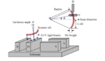
You are currently viewing SemiWiki as a guest which gives you limited access to the site. To view blog comments and experience other SemiWiki features you must be a registered member. Registration is fast, simple, and absolutely free so please,
join our community today!
For the 10nm – 5nm nodes, the leading-edge foundries are designing cells which utilize 6 or 7 metal tracks, entailing a wide metal line for every 4 or 5 minimum width lines, respectively (Figure 1).
Figure 1. Left: a 7-track cell. Right: a 6-track cell.
This is a fundamental vulnerability for lithography, as defocus can change… Read More
It is now time for the EUV community to realize they are caught between the proverbial Scylla and Charybdis. In Greek mythology, the two monsters terrorized ships that were unlucky enough to pass between them. By avoiding one, you approached the other.
S for Scylla, or Stochastics
Scylla was a former beautiful nymph turned into
…
Read More
In the recent DRAM jargon, “1X”, “1Y”, “1Z”, etc. have been used to express all the sub-20 nm process generations. It is almost possible now to match them to real numbers which are roughly the half-pitch of the DRAM active area, such as 1X=18, 1Y ~ 17, etc. At this rate, 14 nm is somewhere around
…
Read More
An update is now available here: Application-Specific Lithography: Patterning 5nm 5.5-Track Metal by DUV
The 5nm foundry (e.g., TSMC) node may see the introduction of 6-track cells (two double-width rails plus four minimum-width dense lines) with a minimum metal pitch in the neighborhood of 30 nm. IMEC had studied a representative… Read More
The stochastic nature of imaging has received a great deal of attention in the area of EUV lithography. The density of EUV photons reaching the wafer is low enough [1] that the natural variation in the number of photons arriving at a given location can give rise to a relatively large standard deviation.
In recent studies [2,3], it … Read More
Self-aligned quadruple patterning (SAQP) is the most widely available technology used for patterning feature pitches less than 38 nm, with a projected capability to reach 19 nm pitch. It is actually an integration of multiple process steps, already being used to pattern the fins of FinFETs [1] and 1X DRAM [2]. These steps, shown… Read More
Moore’s Law has been about device density, specifically transistor density, increasing every certain number of years. Although cost is the most easily grasped advantage, there are two other benefits: higher performance (speed) and reduced power. When these benefits are compromised, they can also pose a scaling limitation.
…
Read More
In a previous article [1], the Rayleigh criterion was mentioned as the resolution limit for the distance between two features. On the other hand, in a following article [2], the minimum pitch was mentioned for the resolution limit for arrayed features. In this article, we reconcile the two by considering gaps between arrayed features,… Read More
State-of-the-art chips will always include some portions which are memory arrays, which also happen to be the densest portions of the chip. Arrayed features are the main targets for lithography evaluation, as the feature pitch is well-defined, and is directly linked to the cost scaling (more features per wafer) from generation… Read More
As any semiconductor process advances to the next generation or “node”, a sticky point is how to achieve the required higher resolution. As noted in another article [1], multipatterning (the required use of repeated patterning steps for a particular feature) has been practiced already for many years, and many have… Read More