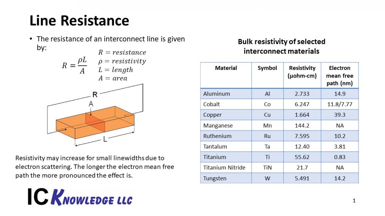
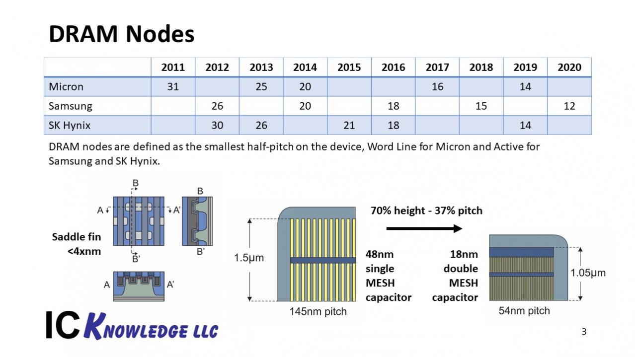
The IEEE Interconnect Technology Conference (IITC): Advanced Metallization Conference was held June 4th through 7th in Santa Clara. Imec presented multiple papers on comparing copper, cobalt and ruthenium interconnect. One paper in particular caught my eye: Marleen H. van der Veen, # N. Heylen, O. Varela Pedreira, S. Decoster,… Read More
Tag: intel
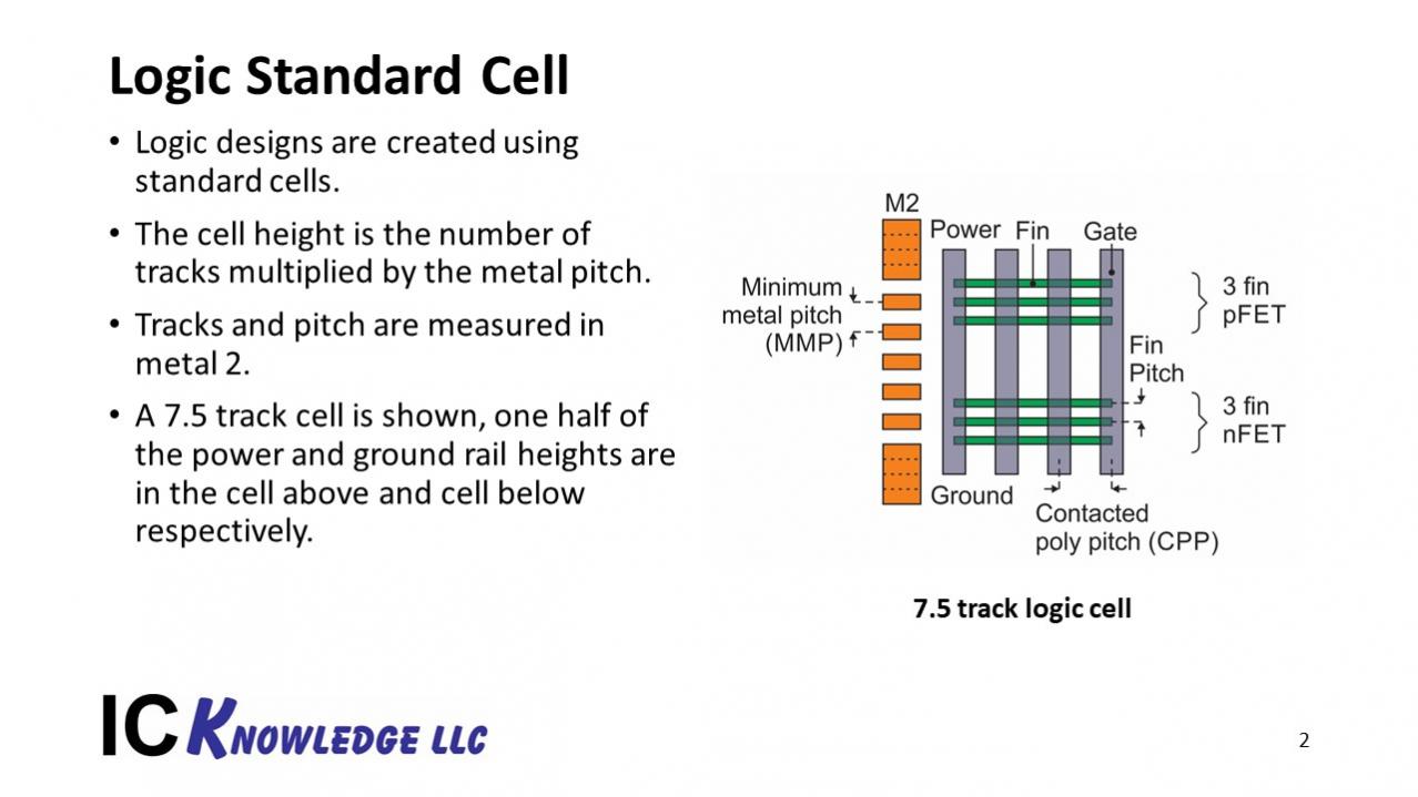
7nm, 5nm and 3nm Logic, current and projected processes
There has been a lot of new information available about the leading-edge logic processes lately. Papers from IEDM in December 2017, VLSIT this month, the TSMC and Samsung Foundry forums, etc. have all filled in a lot of information. In this article I will summarize what is currently known.… Read More
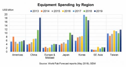
Semiconductor Cycles Always End the Same Way
It appears the current cycle has rolled over? The reason is memory & could be worsened by trade Figuring out length, depth and impact of the downturn? We had said that AMAT “called” the top of the cycle on their last conference call even though they may not think so. Semiconductor cycles always ends the same way. The… Read More
The Rise and Fall of ARM Holdings
Publishing a book on the history of ARM was an incredible experience. In business it is always important to remember how you got to where you are today to better prepare for where you are going tomorrow. The book “Mobile Unleashed” started at the beginning of ARM (Acorn Computer) where a company went from a crazy idea a couple of engineers… Read More
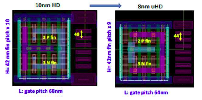
Samsung 10nm 8nm and 7nm at VLSIT
I got a tip sheet today for the upcoming 2018 Symposia on VLSI Technology & Circuits to be held June 19th through 21st in Honolulu, Hawaii. There is some interesting information on Samsung’s 10nm, 8nm and 7nm processes in the tip sheet:… Read More
Intel 10nm Yield Issues
On their first quarter earnings call Intel announced that volume production of 10nm has been moved from the second half of 2018 to 2019 due to yield issues. Specifically, they are shipping 10nm in low volume now, but yield improvement has been slower than anticipated. They report that they understand the yield issues but that improvements… Read More
Data Center Powers Intel but 10NM Still Slow
Intel (INTC) blew away expectations based on strong performance in the data center. Revenues of $16.1B versus street of $15.05B and EPS of $0.93 versus street of $0.72. While revenue was up 9% over prior year, earnings were 50% higher. Guidance is for Q2 revenue of $16.3B and EPS of $0.85 versus street of $15.55B and EPS of $0.81. IOT,… Read More
Cleaning Trends for Advanced Nodes
I was invited to give a talk at the Business of Cleans Conference held by Linx Consulting in Boston on April 9th. I am not a cleans expert but rather was invited more to give an overview talk on process technology trends and the impact on cleans. In this write up I will discuss my presentation. I discussed each of the three main leading-edge… Read More
Intel to buy Micron – Trump Blocks IC Equipment Sales to China – Broadcom Fighting for QCOM
It has been reported over the holiday weekend that Intel is in talks with Micron over a proposed merger that would value Micron at $70 per share in a deal of a combination of stock and cash for Micron shareholders. It is said that the boards of both companies have already approved the deal.
Intel’s CEO Brian Krzanich said, “We… Read More
Vertical Prototyping with Intel FPGAs
It has been an article of faith in the design tools business that there’s little to be gained from targeting market verticals because as far as tools are concerned, all verticals have the same needs. Which is good in some respects; you maximize the breadth of the market to which tooling can appeal. But in so doing the depth of contribution… Read More


