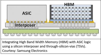
I have been watching the trend for quite some time now that many advanced FinFET designs today are actually 2.5D systems in package. All of these 2.5D silicon interposer-based designs have high-bandwidth memory (HBM) stacks on board. Often there are multiple memory stacks in both 4-high and 8-high configurations. If you follow… Read More
Tag: hbm2
A Future Vision for 3D Heterogeneous Packaging
At the recent Open Innovation Platform® Ecosystem Forum in Santa Clara, TSMC provided an enlightening look into the future of heterogeneous packaging technology. Although the term chiplet packaging is often used to describe the integration of multiple silicon die of potentially widely-varying functionality, this article… Read More
ML and Memories: A Complex Relationship
No, I’m not going to talk about in-memory-compute architectures. There’s interesting work being done there but here I’m going to talk here about mainstream architectures for memory support in Machine Learning (ML) designs. These are still based on conventional memory components/IP such as cache, register files, SRAM and various… Read More
Open-Silicon SiFive and Customizable Configurable IP Subsystems
After 8 SemiWiki years, 4,386 published blogs, and more than 25 million blog views, I can tell you that IP is the most read semiconductor topic, absolutely, and that trend continues. Another correlating trend (from IP Nest) is the semiconductor IP revenue increase in relation to the semiconductor market (minus memory) which more… Read More
RISC-V End to End Solutions for HPC and Networking
Semiconductor IP is one of the more exciting and most viewed topics we cover on SemiWiki, it has been that way since we began in 2011 and that trend will continue indefinitely, my opinion.
Semiconductor IP: Total Blogs: 640: Total Views: 3253751: Average: 5084
Based on the design starts we track, Cloud Computing is a leading semiconductor… Read More
Custom SoC Platform Solutions for AI Applications at the TSMC OIP
The TSMC OIP event is next week and again it is packed with a wide range of technical presentations from TSMC, top semiconductor, EDA, and IP companies, plus long time TSMC partner and ASIC provider Open-Silicon, a SiFive Company. You can see the full agenda HERE.
AI is revolutionizing and transforming virtually every industry… Read More
Welcome DDR5 and Thanks to Cadence IP and Test Chip
Will we see DDR5 memory (device) and memory controller (IP) in the near future? According with Cadence who has released the first test chip in the industry integrating DDR5 memory controller IP, fabricated in TSMC’s 7nm process and achieving a 4400 megatransfers per second (MT/sec) data rate, the answer is clearly YES !
Let’s come… Read More
What does a Deep Learning Chip Look Like
There’s been a lot of discussion of late about deep learning technology and its impact on many markets and products. A lot of the technology under discussion is basically hardware implementations of neural networks, a concept that’s been around for a while.
What’s new is the compute power that advanced semiconductor technology… Read More
High Performance Ecosystem for 14nm-FinFET ASICs with 2.5D Integrated HBM2 Memory
High Bandwidth Memory (HBM) systems have been successfully used for some time now in the network switching and high-performance computing (HPC) spaces. Now, adding fuel to the HBM fire, there is another market that shares similar system requirements as HPC and that is Artificial Intelligence (AI), especially AI systems doing… Read More
FinFET ASICs for Networking, Data Center, AI and 5G
On the heels of successful seminars in Tokyo and Shanghai, eSilicon is starting the new year back in the cloud with a webinar version of the live events for those, like myself, who could not attend. The webinar will compress the 3 hour live event into 60 minutes which will provide a great place to start a conversation on your next chip… Read More


