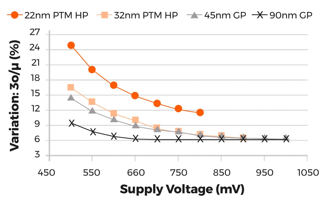
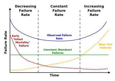
At Intel back in the late 1970’s we wanted to know what process corner each DRAM chip and wafer was trending at so we included a handful of test transistors in the scribe lines between the active die. Having test transistors meant that we could do a quick electrical test at wafer probe time to measure the P and N channel transistor… Read More
Tag: finfet
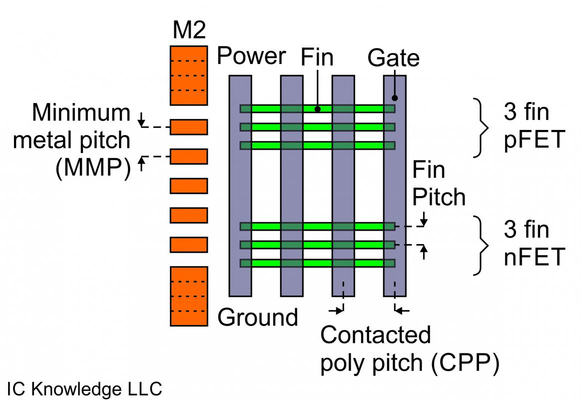
IEDM 2017 – Leti Gate-All-Around Stacked-Nanowires
At IEDM in December I had a chance to interview Thomas Ernst about the paper “Performance and Design Considerations for Gate-All-around Stacked-NanoWires FETs” by Leti and STMicroelectonics.
Leti published the first stacked nanowire in 2006, it was very new then, now stacked nanowire/nanosheets are starting… Read More
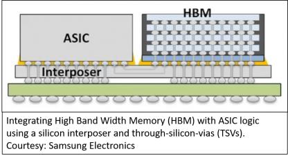
High Performance Ecosystem for 14nm-FinFET ASICs with 2.5D Integrated HBM2 Memory
High Bandwidth Memory (HBM) systems have been successfully used for some time now in the network switching and high-performance computing (HPC) spaces. Now, adding fuel to the HBM fire, there is another market that shares similar system requirements as HPC and that is Artificial Intelligence (AI), especially AI systems doing… Read More
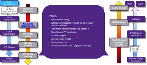
Achieving ISO 26262 Certification with ASIL Ready IP
According with McKinsey, “analysts predict revenue growth for advanced driver assistance systems (ADAS) to be up to 29 percent, giving the segment one of the highest growth rates in the automotive and related industries.” Design cycle in automotive segment is much longer than in segments like mobile, PC or consumer. If you expect… Read More
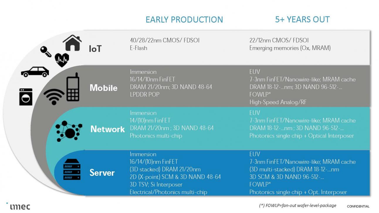
IEDM 2017 – imec Charting the Future of Logic
At the IEDM 2017, imec held an imec technology forum and presented several papers, I also had the opportunity to interview Anda Mocuta director of technology solutions and enablement. In this article I will summarize the keys points of what I learned about the future of logic. I will follow this up with a later article covering memory.… Read More
Advanced ASICs – It Takes an Ecosystem
I remember the days of the IDM (integrated device manufacturer). For me, it was RCA, where I worked for 15 years as the company changed from RCA to GE and then ultimately to Harris Semiconductor. It’s a bit of a cliché, but life was simpler then, from a customer point of view at least. RCA did it all. We designed all the IP, did the physical… Read More
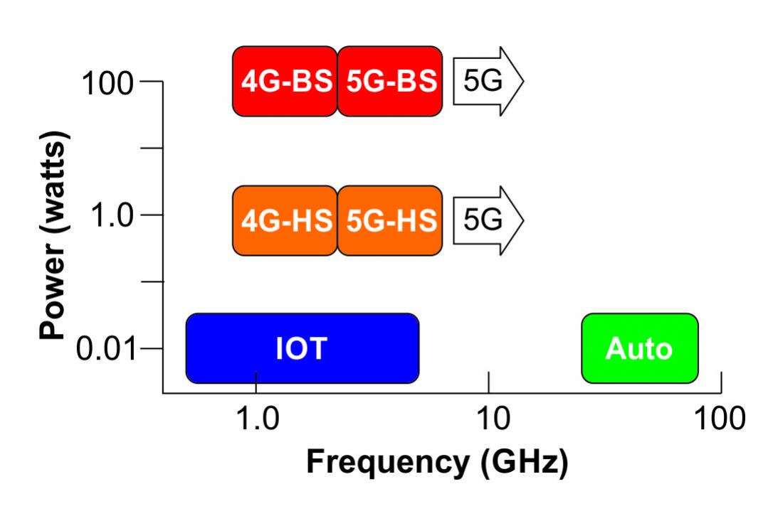
GLOBALFOUNDRIES RF Leadership
“Mobile is the largest platform ever built by humanity”, Christiano Amon, Executive Vice President, Qualcomm Technologies, Inc. and President, Qualcomm CDMA Technologies speaking at the GLOBALFOUNDRIES Technologies Conference (GTC) 2017.… Read More
TechCon: See ANSYS and TSMC co-present
ANSYS and TSMC will be co-presenting at ARM TechCon on Multiphysics Reliability Signoff for Next Generation Automotive Electronics Systems. The event is on Thursday October 26th, 10:30am-11:20am in Grand Ballroom B.
You can get a free Expo pass which will give you access to this event HERE and see the session page for the event … Read More
TSMC Teamwork Translates to Technical Triumph
Most people think that designing successful high speed analog circuits requires a mixture of magic, skill and lots of hard work. While this might be true, in reality it also requires a large dose of collaboration among each of the members of the design, tool and fabrication panoply. This point was recently made abundantly clear … Read More
Semiconductor Device Physics, Lab in a Box
One of my favorite classes in college was the lab exercise, mostly because we actually got to use real electronics and then measure something, finally writing it up in our lab notebooks. The issue today is that a college student taking Electrical Engineering probably doesn’t have much access to 10nm FinFET silicon for use… Read More


