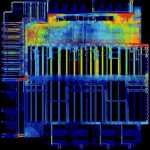
Siemens Mentor recently announced PAVE360™, a very cool comprehensive pre silicon simulation environment. Autonomous cars are very popular here in Silicon Valley and quite safe on the highways since the average speed is 25mph (horrible traffic). In the city you need autonomous parking unless you want to waste precious time … Read More
Tag: eda
The New Silvaco CEO is SURGING!
One of my great pleasures in the semiconductor industry is meeting the people who have brought us to where we are today, at the forefront of modern life. One of those people is Babak Taheri, now CEO of Silvaco who I spent time with yesterday. Babak started in semiconductors around the same time I did 30+ years ago. He has a PhD in EECS and… Read More
Chapter Nine – Specialization Inhibits System Level Optimization
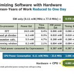
Solving critical customer problems sometimes isn’t enough. One of my most interesting experiences came during the development and rollout of a product that was designed to optimize integration of hardware and embedded software. In this case, the product performed exactly as planned but the plan ignored the organizational… Read More
Webinar – Fabless: The Transformation of the Semiconductor Industry 2019 Update!
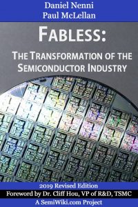
As more than 343 people (and counting) know, we will be releasing the 2019 updated PDF version of our first book “Fabless: The Transformation of the Semiconductor Industry” via handout at a live webinar. The response has been overwhelming and I want to personally thank you. The webinar will be a brief overview of the book with a question… Read More
Silvaco Talks Atoms to Systems – Where to Next?
At the ES Design West event in San Francisco last week Silvaco’s CTO and EVP of Products, Babak Taheri, gave a presentation titled, “Next Generation SoC Design: From Atoms to Systems”. The time slot for the talk was only 30-minutes which is simply not enough to discuss all the technology Silvaco is providing now. I had not looked closely… Read More
WEBINAR: Eliminating Hybrid Verification Barriers Through Test Suite Synthesis
I’ve been following the evolution of the verification space for a very long time including several stints consulting to formal verification companies. It has always been interesting to me to see how so many diverse verification techniques emerge and been used, but without much unification of the approaches. With the emergence… Read More
Webinar: Addressing Multiphysics Challenges in 7nm FinFET Designs
EDA is big on growth through acquisition, being acquired many times throughout my career I know this by experience. In fact, we have a wiki that tracks EDA Mergers and Acquisitions and it is the most viewed wiki on SemiWiki.com with 101,918 views thus far.
In March of 2017 ANSYS acquired CLK Design Automation which did timing variation… Read More
Samsung IEDM 2018 Keynote and the Foundry Business
IEDM is a premier semiconductor conference so it was certainly appropriate for Samsung to do the keynote since they are the largest and one of the most innovative semiconductor companies in the world, absolutely.
Samsung is also one of the more interesting semiconductor companies since they do it all: chip design, semiconductor… Read More
Q4 Hiring remains strong Outlook for Q1 2019
Things are going quite well in the Valley, ESPECIALLY if traffic is any indication. I still remember the BUST with the empty office buildings and light traffic, back in the early 2000’s…while I wish for traffic like that always, I certainly prefer the busy times, guess you cannot have it all. The more traffic, the more jobs; they invariably… Read More
TSMC and Synopsys are in the Cloud!
EDA has been flirting with the cloud unsuccessfully for many years now and it really comes down to a familiar question: Who can afford to spend billions of dollars on data center security? Which is similar to the question that started the fabless transformation: Who can afford to spend billions of dollars on semiconductor manufacturing… Read More


