Chiplets dominate semiconductor industry conversations right now – and after the recent Chiplet Summit, we expect the intensity to go up a couple of notches. One company name often heard is Blue Cheetah, and we had the opportunity to sit down with them recently to discuss their views and their just-announced design win at Tenstorrent.… Read More

Tag: chiplets
How Disruptive will Chiplets be for Intel and TSMC?

Chiplets (die stacking) is not new. The origins are deeply rooted in the semiconductor industry and represent a modular approach to designing and manufacturing integrated circuits. The concept of chiplets has been energized as a response to the recent challenges posed by the increasing complexity of semiconductor design. … Read More
Keysight EDA Connect World Tour

Video webinars are a main staple to learn what’s new about EDA tools and methodologies, but there’s nothing quite like meeting in person, where you can ask questions and gauge the expertise of the presenters. I was delighted to learn that Keysight is planning a literal world tour to update EDA customers and prospects on what they … Read More
Alphawave Semiconductor Powering Progress
Do you know who had another great year? Alphawave Semi did. Despite being relatively young in the industry (founded in 2017), the company has quickly gained recognition for its advancements in high-speed connectivity solutions.
They specialize in developing high-speed connectivity solutions for Data centre, AI, 5G wireless… Read More
2024 Big Race is TSMC N2 and Intel 18A

There is a lot being said about Intel getting the lead back from TSMC with their 18A process. Like anything else in the semiconductor industry there is much more here than meets the eye, absolutely.
From the surface, TSMC has a massive ecosystem and is in the lead as far as process technologies and foundry design starts but Intel is … Read More
Will Chiplet Adoption Mimic IP Adoption?
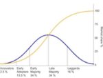
If we look at the semiconductor industry expansion during the last 25 years, adoption of design IP in every application appears to be one of the major factors of success, with silicon technology incredible development by a x100 factor, from 250nm in 2018 to 3nm (if not 2nm) in 2023. We foresee the move to chiplet-based architecture… Read More
Unleashing the 1.6T Ecosystem: Alphawave Semi’s 200G Interconnect Technologies for Powering AI Data Infrastructure
In the rapidly evolving landscape of artificial intelligence (AI) and data-intensive applications, the demand for high-performance interconnect technologies has never been more critical. Even the 100G Interconnect is already not fast enough for infrastructure applications. AI applications, with their massive datasets… Read More
Successful 3DIC design requires an integrated approach

While the leap from traditional SoC/IC designs to Three-Dimensional Integrated Circuits (3DICs) designs brings new benefits and opportunities, it also introduces new challenges. The benefits include performance, power efficiency, footprint reduction and cost savings. The challenges span design, verification, thermal… Read More
Podcast EP193: A Look at the Engineering Tracks for DAC 2024 with Frank Schirrmeister
Dan is joined by Frank Schirrmeister. Frank is vice president of solutions and business development at Arteris. He leads activities for industry verticals, including automotive and enterprise computing and technology horizontals like artificial intelligence, machine learning, and safety. For DAC 2024, Frank is the vice… Read More
Arm Total Design Hints at Accelerating Multi-Die Activity

I confess I am reading tea leaves in this blog, but why not? Arm recently announced Arm Total Design, an expansion of their Compute Subsystems (CSS) offering which made me wonder about the motivation behind this direction. They have a lot of blue-chip partners lined up for this program yet only a general pointer to multi-die systems… Read More