You are currently viewing SemiWiki as a guest which gives you limited access to the site. To view blog comments and experience other SemiWiki features you must be a registered member. Registration is fast, simple, and absolutely free so please,
join our community today!
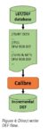
GDS and LEF/DEF each came about to support data exchange in different types of design flows, custom layout and place & route respectively. GDS (or stream format) was first created in the late 1970s to support the first generation of custom IC layout tools, such as Calma’s GDSII system. Of course, the GDS format has been updated… Read More
All semiconductor design work today rests on the three-legged stool of Foundries, EDA Tools and Designers. Close collaboration between the three make possible the successful completion of ever more complex designs, especially those at advanced nodes. Perhaps one of the most critical intersections of all three is during physical… Read More
Having the right tool for the job at hand is always a joy, and when your IC project involves RTL code, gates, transistors and even parasitic interconnect, then you need some EDA tool help for debugging and finding out why your design behaves the way it is. An FAE named Sujit Roy did a conference call with me last week to show what StarVision… Read More
Physical verification is an important and necessary step in the process to tapeout an IC design, and the foundries define sign-off qualification steps for:
- Physical validation
- Circuit validation
- Reliability verification
This sounds quite reasonable until you actually go through the steps only to discover that some of the … Read More
Calibre was a big game changer for DRC users when it first came out. Its hierarchical approach dramatically shortened runtimes with the same accuracy as other existing, but slower, flat tools. However, one unsung part of this story was that getting Calibre up and running required minimal effort for users. Two things are required… Read More
A product launch nowadays demands shorter runway. SoC designers challenges are not so much in facing the unavailability of proven design capture methodologies or IP’s that could satisfy their product requirements, but more so in orchestrating the integration of all those components to deliver the targeted functionalities… Read More
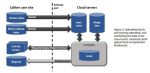
It was inevitable that EDA applications would meet the cloud. EDA has a long history of creating some of the most daunting compute challenges. This arises from employing current generation chips to design the next generation chips. Despite growing design complexity, many tools have kept pace and even reduced runtimes from generation… Read More
This will be one of the more interesting Mentor User Group Meetings now that the Siemens acquisition has fully taken effect and the new management team is in place. The Mentor User Conference is at the Santa Clara Marriott, Santa Clara, California on May 2, 2019 from 9:00 am to 6:00pm.
Remember, in 2017 Siemens acquired Mentor Graphics… Read More
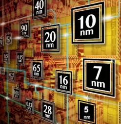
Last week TSMC announced the availability of its complete 5nm design infrastructure that enables SoC designers to implement advanced mobile and high-performance computing applications for the emerging 5G and AI driven markets. This fifth generation 3D FinFET design infrastructure includes technology files, PDKs (Process… Read More
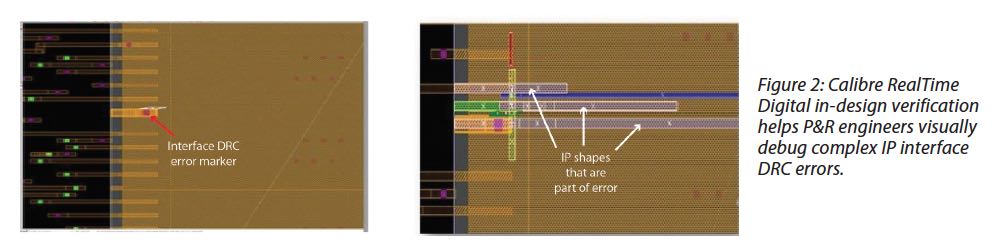
When floor planning (FP) and place & route (P&R) tools took over from custom layout tools for standard cell based designs, life became a lot better for designers of large digital chips. The beauty of the new flows was that all the internals of the standard cells and many IP blocks were hidden from view, lightening the load … Read More