You are currently viewing SemiWiki as a guest which gives you limited access to the site. To view blog comments and experience other SemiWiki features you must be a registered member. Registration is fast, simple, and absolutely free so please,
join our community today!
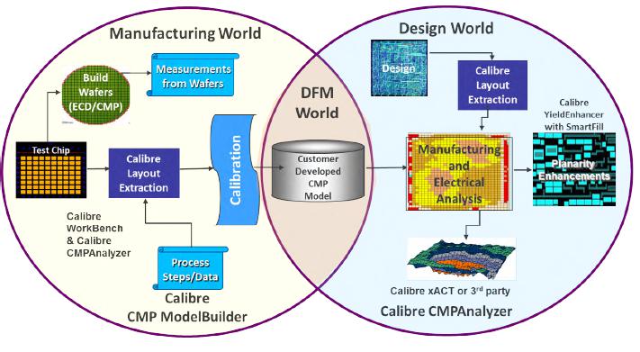
CMP (Chemical Mechanical Planarization or also known as Chemical Mechanical Polishing) is a wafer fabrication step applied generally after a chemical deposition –intended to smoothen and to flatten (planarize) wafer surfaces with the combination of chemical and mechanical forces. Developed at IBM and since its introduction… Read More
This is the eighteenth in the series of “20 Questions with Wally Rhines”
Gerry Hsu’s departure from Cadence to form Avanti (originally named ArcSys) is chronicled in legal testimony as accusations of theft of software were followed by legal battles, financial awards and even prison terms. Mentor and Synopsys were… Read More
Light is a form of energy. It reveals an object’s color and shape through the refraction (passing through light) or the reflection (bouncing back light) of its beam. While photon is the smallest measure of light, the term photonicscan be defined as the science and technology of generating, controlling, and detecting photons. … Read More
This is the fourteenth in the series of “20 Questions with Wally Rhines”
I joined Mentor Graphics (now Mentor, A Siemens Business), in late 1993. Tom Engibous, one of my direct reporting people at TI, was promoted to replace me as head of the Semiconductor business of TI and I moved on to what I knew would be a real challenge,… Read More
During the design cycle as tape out approaches, time pressure usually goes up dramatically. To make matters worse the design itself is much larger, because all the block level work is done and there is a requirement to work with the entire database. It feels like it’s time to put aside the garden trowel and start using a steam shovel.… Read More
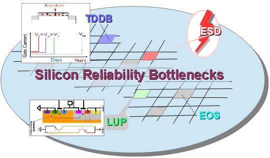
Advanced process technology offers both device and interconnect scaling for increased design density and higher performance while invoking also significant implementation complexities. Aside from the performance, power and area (PPA) aspects, designer is getting entrenched with the need of tackling more reliability … Read More
Design process retargeting is acommon recurrence based on scaling orBOM(Bill-Of-Material) cost improvement needs. This occursnot only with the availability of foundry process refresh to a more advanced node,but also to any new derivative process node tailored towards matching design complexity, power profile or reliability… Read More
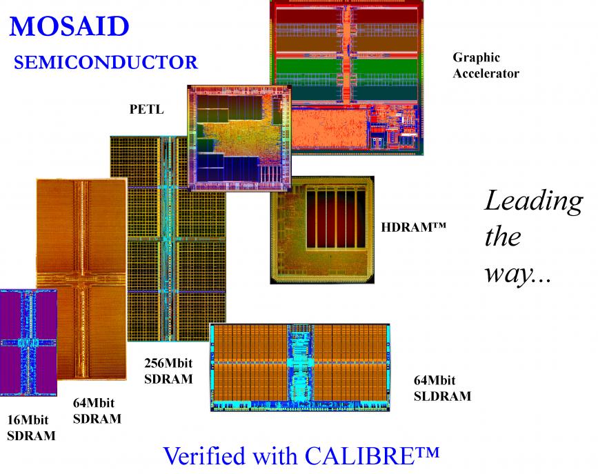
Being new in Ottawa and trying to get some momentum towards automation in full custom layout I was telling industry people that I am interested to work with everybody to move this agenda forward. My Director of Engineering at that time, Peter Gillingham, took me to visit Carleton University in Ottawa. One of his professor friends,… Read More
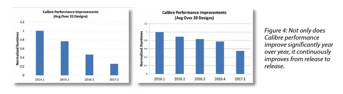
One might be tempted to think that technology driven gains in computer performance might be enough to keep up with the needs of design and verification tools. We know that design complexity is increasing at a rate predicted by Moore’s Law. We also know that the performance of the computers used during IC development benefit from … Read More
Back in the early 1980’s during the nascent years of electronic design automation (EDA), I worked at Texas Instruments supporting what would become their merchant ASIC business. Back then, life was a bit different. The challenge we faced was to make our ASIC library available on as many EDA flows as we could to give as many users as… Read More