You are currently viewing SemiWiki as a guest which gives you limited access to the site. To view blog comments and experience other SemiWiki features you must be a registered member. Registration is fast, simple, and absolutely free so please,
join our community today!
TI has parlayed its heritage in digital signal processing and long-term relationships with mobile device makers into a leadership position in mobile SoCs. They boast a relatively huge portfolio of design wins thanks to being the launch platform for Android 4.0. On the horizon, the next generation OMAP 5 could change the entire… Read More
I Love DACby Paul McLellan on 04-13-2012 at 1:16 pmCategories: EDA, Events
For the fourth year Atrenta, Cadence and Springsoft are jointly sponsoring the “I LOVE DAC” campaign. In case you have been hibernating all winter, DAC is June 3-7th in San Francisco at the Moscone Center.
There are two parts to “I LOVE DAC”. First, if you register by May 15th (and they haven’t all… Read More
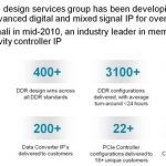
The press release about ONFI 3.0 support was launched by Cadence at the beginning of this year. It was a good illustration of Denali, then Cadence, long term commitment to Nand Flash Controller IP support. The ONFI 3 specification simplifies the design of high-performance computing platforms, such as solid state drives and enterprise… Read More
Recently I was researching the keynote speeches of isQED (International Society for Quality Electronic Design) Symposium 2012 and saw the very first, great presentation, “Taming the Challenges in Advanced Node Design” by Tom Beckley, Sr. VP at Cadence. I know Tom very well as I have worked with him and I admire his knowledge, authority… Read More
Before I get too snarky here, I would like to thank Synopsys for the invitation to SNUG 2012 and including me with the professional editors at a 75 minute roundtable discussion with Synopsys CEO Aart de Geus. While Aart is not my favorite big EDA CEO (Wally Rhines of Mentor bought me lunch and returns my email), he is definitely the most… Read More
Lip-Bu Tan, the CEO of Cadence, has been named by the Singapore Business Awards as Outstanding CEO (overseas) last week. These awards were launched in 1985 by the Business Times and DHL, so this year is the 27th year of the award, created to recognize business leaders in Singapore and abroad.
As it happens, Cadence flew me first class… Read More
The two large EDA companies offering SOC prototyping with FPGA-based boards are Synopsys and Cadence, however there’s a smaller vendor called Polaris Design Systems that also have a product in this important design verification category. I spoke on Wednesday with Rahm Shastry, CEO of Polaris to learn more about this company… Read More
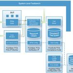
The launch from Cadence of the PCI Express 3.0 Controller IP was officially done about one year ago, and demonstrated at the June 2011 PCI-SIG Developer’s Conference, where Cadence Design IP for PCI Express 3.0 controller IP implemented as a high-performance, dual-mode, 128-bit data-path, x8 PCI Express 3.0 controller… Read More
John Stabenow is the marketing group director at Cadence for the Virtuoso products and it has been awhile since we last talked, so we met for lunch on Friday at McMenamins in a city called West Linn, half-way between where we both live in Oregon. I had blogged about Interoperability at DAC 2010 and we had a public exchange at Chip Design… Read More
There were three keynotes at CDNLive this morning, and one theme ran through them: collaboration. In fact there was one specific instance of collaboration that all three people mentioned. Taping out an ARM Cortex-A15 in TSMC 20nm technology using a Cadence tool flow.
Lip-Bu, Cadence’s CEO, went first. He had some numbers… Read More