You are currently viewing SemiWiki as a guest which gives you limited access to the site. To view blog comments and experience other SemiWiki features you must be a registered member. Registration is fast, simple, and absolutely free so please,
join our community today!
The most viewed blogs I write for SemiWiki are consistently blogs comparing the four leading edge logic producers, GLOBALFOUNDRIES (GF), Intel, Samsung (SS) and TSMC. Since the last time I compared the leading edge new data has become available and several new processes have been introduced. In this blog I will update the current… Read More
This year the Advanced Lithography Conference felt very different to me than the last couple of years. I think it was Chris Mack who proclaimed it the year of Stochastics. EUV has dominated the conference for the last several years but in the past the conversation has been mostly centered on the systems, system power and uptime.
I … Read More
I was invited to present at Nikon’s LithoVision event held the day before the SPIE Advanced Lithography Conference in San Jose. The following is a write up of the talk I gave. In this talk I discuss the three main segments in the semiconductor industry, NAND, DRAM and Logic and how technology transitions will affect lithography.… Read More
At IEDM in December I had a chance to interview Thomas Ernst about the paper “Performance and Design Considerations for Gate-All-around Stacked-NanoWires FETs” by Leti and STMicroelectonics.
Leti published the first stacked nanowire in 2006, it was very new then, now stacked nanowire/nanosheets are starting… Read More
I was invited to give a talk at the ISS conference on the Impact of EUV on the Semiconductor Supply Chain. The ISS conference is an annual gathering of semiconductor executives to review technology and global trends. In this article I will walk through my presentation and conclusions.… Read More
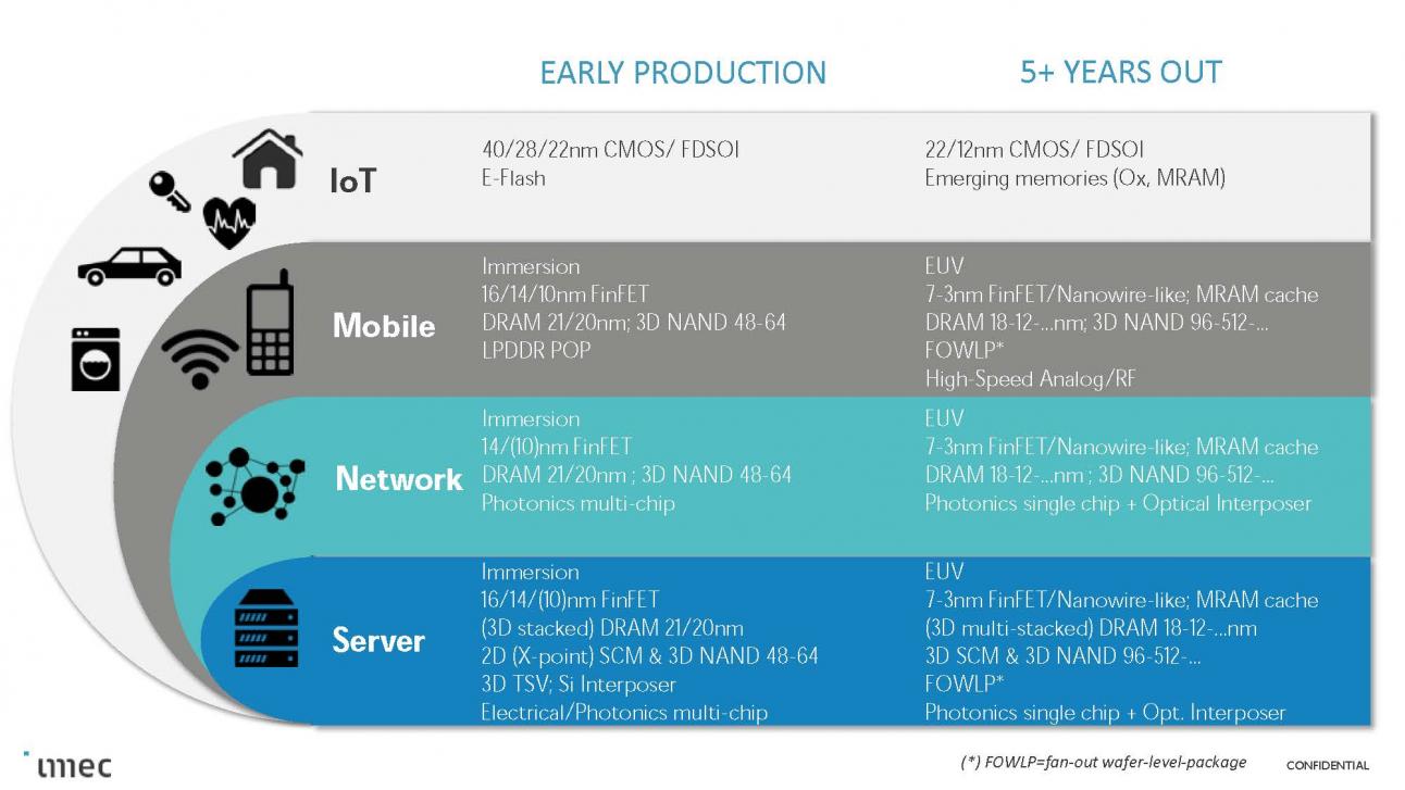
At the IEDM 2017, imec held an imec technology forum and presented several papers, I also had the opportunity to interview Anda Mocuta director of technology solutions and enablement. In this article I will summarize the keys points of what I learned about the future of logic. I will follow this up with a later article covering memory.… Read More
For Halloween this week we thought it would be appropriate to talk about things that strike fear into the hearts of semiconductor makers and process engineers toiling away in fabs. Do I want to do multi-patterning with the huge increase in complexity, number of steps, masks and tools or do I want to do EUV with unproven tools, unproven… Read More
At the imec technology forum held at SEMICON West, Martin Van Den Brink, President and CTO of ASML presented on the latest developments on EUV. I also had an opportunity to sit down with Mike Lercel, ASML Director of Strategic Marketing for an interview.… Read More
At SEMICON West I attended the imec technology forum where Zsolt Tokei presented “How to Solve the BEOL RC Dilemma” and the SEMICON Economics of Density Scaling session where Larry Clevenger of IBM presented “Interconnect Scaling Strategic for Advanced Semiconductor Nodes”. I also had the opportunity… Read More
Samsung recently held a meeting where they laid out a detailed roadmap for their foundry business. On Tuesday June 1st, Daniel Nenni and myself had an interview with Kelvin Low, senior director of foundry marketing and business development to discuss the details of Samsung’s plans.… Read More