You are currently viewing SemiWiki as a guest which gives you limited access to the site. To view blog comments and experience other SemiWiki features you must be a registered member. Registration is fast, simple, and absolutely free so please,
join our community today!
The semiconductor industry is experiencing rapid evolution, driven by the proliferation of IoT applications, image sensors, photonics, MEMS applications, 3DIC and other emerging technologies. This growth has dramatically increased the complexity of integrated circuit (IC) design. One aspect of this complexity is the … Read More
In a DACtv session on July 22, 2024, Rich Goldman from Ansys discussed the partnership with NVIDIA, focusing on accelerating engineering simulations and visualizing 3D IC designs in Omniverse. The collaboration, outlined in six pillars defined by NVIDIA CEO Jensen Huang, leverages NVIDIA’s GPUs and Grace CPUs to enhance… Read More
This year’s live semiconductor ecosystem conferences have been well attend and I expect the same for #61DAC next week. I will be at the conference from Sunday afternoon to Wednesday evening, if you would like to meet let me know. Networking is an important part of the semiconductor ecosystem so let’s make it happen.… Read More
We have been working with Ansys since SemiWiki was founded in 2011. It has been a richly rewarding relationship in all regards. I always say the semiconductor industry is filled with the most intelligent people in the world and Ansys is an excellent proof point. I have known John Lee for 30+ years and he is one of my trusted few, absolutely.… Read More
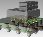
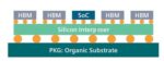
One of the most promising advancements in the semiconductor field is the development of 3D Integrated Circuits (3D ICs). 3D ICs enable companies to partition semiconductor designs and seamlessly integrate silicon Intellectual Property (IP) at the most suitable process nodes and processes. This strategic partitioning yields… Read More
Highlights:
- Ansys CTO Prith Banerjee will be delivering the Visionary Speaker opening address on Tuesday 11th
- There will be technical presentations every hour in the Ansys Booth Theater (#1539)
- Get yourself a complimentary sit-down breakfast and a discussion on automotive electronics by registering for the Ansys DAC
…
Read More
As one of the world’s leading chip foundries, Samsung occupies a vital position in the semiconductor value chain. The annual Samsung Advanced Foundry Ecosystem (SAFE™) Forum is a must-go event for semiconductor and electronic design automation (EDA) professionals. Ajei Gopal, President and CEO of Ansys, has the honor of delivering… Read More
At the recent Synopsys Users Group Meeting (SNUG) I had the honor of leading a panel of experts on the topic of chiplets. One of those panelists was John Lee, Head of Electronics, Semiconductors and Optics at Ansys.
How is the signoff flow evolving and what is being done to help mitigate the growing signoff complexity challenge?
With… Read More
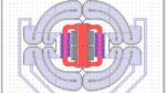
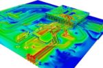
Multiphysics simulation is the process of computational methods to model and analyze a system to understand its response to different physical interactions like heat transfer, electromagnetic fields, and mechanical structures. Using this technique, designers can generate physics-based models and analyze the behavior… Read More
I just did a Google search for “3D IC”, and was stunned to see it return a whopping 476,000 results. This topic is trending, because more companies are using advanced IC packaging to meet their requirements, and yet the engineers doing the 3D IC design have new challenges to overcome. One of those challenges is creating… Read More