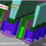
While FinFET yield controversy is going on, I see a lot being done to improve that yield by various means. One prime trend today, it must be, it’s worthwhile, is to pull up various signoffs as early as possible during the design cycle. And DFM signoff is a must with respect to yield of fabrication. This reminds me about my patents filed… Read More
Tag: 14nm
TSMC Breaks More Records in Q3 2014!
As previously predicted TSMC is having another record breaking SoC quarter. TSMC is my favorite economic bellwether and from what I can see the semiconductor industry will continue to grow this year and next at a rapid rate thanks to TSMC and the fabless semiconductor ecosystem:
We have set a new record of revenue and profitability… Read More
The Apple Samsung TSMC Intel 14nm Mashup!
One of the strengths of the fabless semiconductor ecosystem is competition since it keeps innovation high and prices low. One of the challenges of fostering competition is that you have to make good on a threat of using a competing product during a pricing negotiation. Well, in my opinion, for the next version of the iPhone, Apple… Read More
GlobalFoundries and Samsung at ARM
It was back in April that GlobalFoundries and Samsung announced that GF would license Samsung’s 14nm process to run in their Fab8 in upstate New York. Since then there has not really been any news and of course those of us that follow the foundry industry wondered to what extent there was real substance to the agreement or if … Read More
ANSYS Tools Shine at FinFET Nodes!
In the modern semiconductor ecosystem we are seeing rapid advancement in technology breaking past once perceived limits; 28nm, 20nm, 16-14nm, 10nm and we are foreseeing 7nm now. Double and multi-patterning are already being seen along with complex FinFET structures in transistors to gain the ultimate advantages in PPA from… Read More
Who Will Lead at 10nm?
There has been a lot of discussion on SemiWiki lately around 14nm FinFET technology and who really leads and by how much. I thought it would be interesting to review some process metrics for previous technology generation and then make some forecasts around 10nm.
The focus of this article will be Intel, TSMC and Global Foundries/Samsung… Read More
Place & Route with FinFETs and Double Patterning
Place & route in the 16/14nm era requires a new approach since it is significantly more complex. Of course, every process generation is more complex than the one before and the designs are bigger. But modern processes have new problems. The two biggest changes are FinFETs and double patterning.
FinFETs, as I assume you know,… Read More
Samsung 14nm FinFET Design with Cadence Tools
The first consumer products with 20nm processing are arriving in 2014 like the 2 billion transistor A8 chip in the iPhone 6, however at the 14nm node there are new designs underway to continue the trend of Moore’s Law. To get a better feel for the challenges of designing with 14nm FinFET technology I watched a 23 minute video … Read More
USB 3.0 IP on FinFET may stop port pinching
Sometimes a standard is a victim of its own success, at least for a while as the economics catch up to the technology. When a standard like USB 3.0 is announced, with a substantial performance increase over USB 2.0, some of the use cases come on board right away. Others, where vendors enjoy a decent ROI with good-enough performance,… Read More
SEMulator3D: GlobalFoundries Process Variation Reduction
At SEMICON last month, Rohit Pal of GlobalFoundries gave a presentation on their methodology for reducing process variation. It was titled Cpk Based Variation Reduction: 14nm FinFET Technology.
Capability indices such as Cpk is a commonly used technique to assess the variation maturity of a technology. It looks at a given parameter’s… Read More


