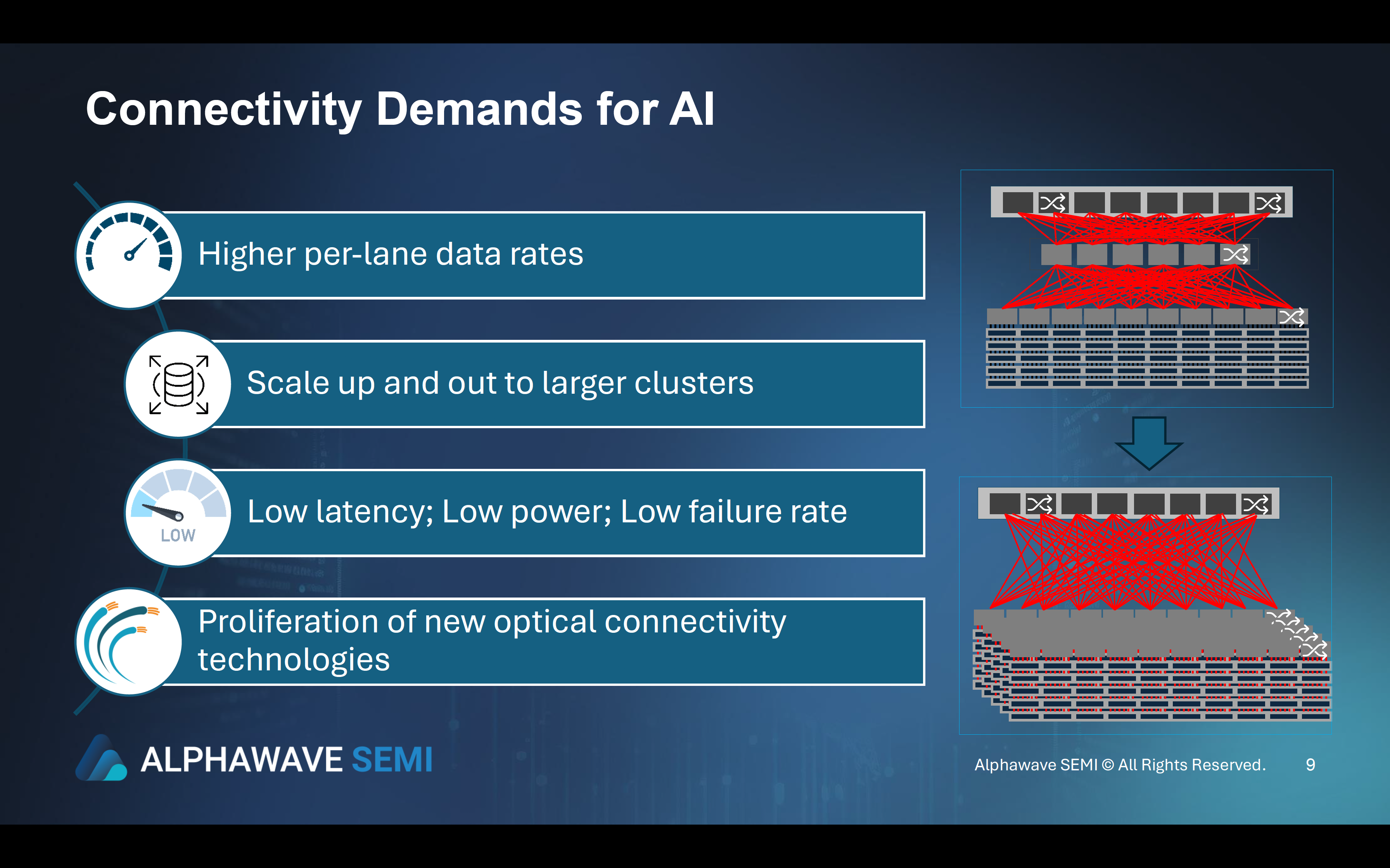
Artificial intelligence (AI) is driving a transformation in data center infrastructure, necessitating cutting-edge technologies to meet the growing demands of AI workloads. As AI systems scale up and out, next-gen compute servers, switches, optical-electrical links, and flexible, redundant networking solutions are crucial. Key innovations—such as advanced connectivity technologies, custom silicon solutions via chiplets, and the proliferation of optical connectivity—are redefining how AI clusters are deployed and operated.
Tony Chan Carusone, CTO at Alphawave Semi gave a talk on this subject at the AI Hardware and Edge AI Summit held in September 2024.
Connectivity Technologies: Enabling Scalable AI Clusters
Scaling AI clusters, whether housed in a single data center or distributed across multiple locations, hinges on high-performance connectivity technologies. AI’s front-end networks, handling data flow, and back-end ML networks, processing large-scale AI computations, require low-latency, high-speed communication. This is increasingly supported by optical-electrical links and flexible, redundant networking, ensuring smooth operation even as demands grow.

A key innovation is the shift from copper-based systems to advanced optical connectivity solutions like pluggable optical modules and co-packaged optics (CPO). These technologies boost performance by reducing latency and increasing bandwidth, critical for AI tasks requiring rapid data exchange.
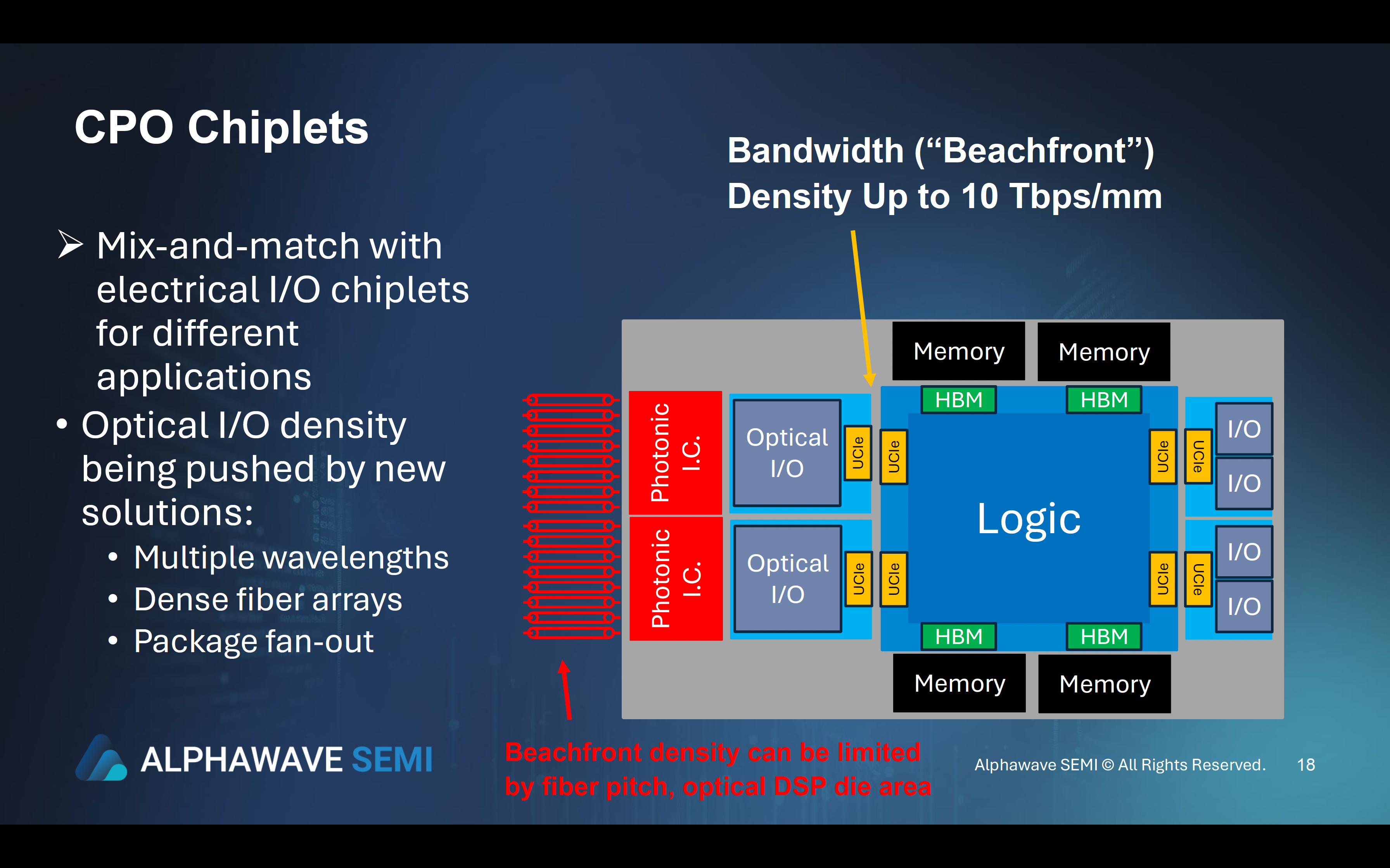
CPO integrates miniature optical engines directly into chip packages, replacing electrical interconnects with optical fiber. Combined with electrical I/O chiplets, CPO chiplets offer a mix-and-match solution optimized for different applications, enhancing AI processing speed and efficiency.

Chiplets: Optimized Silicon Solutions for AI Workloads
As AI workloads grow more complex, custom silicon solutions are essential. Chiplets enable specialized hardware tailored to specific AI tasks. Built on low-cost substrates, chiplets enhance affordability without sacrificing performance. Their flexible configurations help data centers meet diverse computational needs.
The chiplet ecosystem, built around die-to-die interfaces like Universal Chiplet Interconnect Express (UCIe), enables seamless communication between I/O, compute, and memory chiplets. For instance, I/O chiplets may feature multi-standard SerDes with controllers for PCIe Gen6, CXL 3.0, or 112Gbps Ethernet, while compute chiplets utilize Arm-based cores for high-performance processing. Memory expansion chiplets with low-latency DDR or HBM ensure faster data access, further enhancing AI performance.
Scaling Performance Affordably and Efficiently
The modular nature of chiplets allows for scalable performance at lower costs. Traditional monolithic chips are expensive and time-consuming to develop, but chiplets, with pre-validated reusable components, reduce development timelines and production costs. This is crucial for AI-driven industries, where efficiency and faster time-to-market are essential.
Chiplets also help manage power consumption—important as data centers scale. Innovations in die-to-die interfaces address challenges related to signal and power integrity, such as crosstalk and interconnect losses. Advances in power delivery and packaging technology, along with improved clocking solutions, are also increasing efficiency in dense signal routing and clock/data alignment.
The Rise of Optical Connectivity in AI Infrastructure
Optical connectivity technologies, particularly within chiplet ecosystems, are transforming the AI data center landscape. CPO and high-density optical I/O solutions are pushing the boundaries of AI clusters’ capabilities. By integrating optical components directly into chip designs, AI systems can handle greater data volumes with lower latency and increased energy efficiency.
Dense fiber arrays, multiple wavelengths, and advanced fan-out techniques ensure that optical I/O meets the increasing data demands of AI. These innovations not only improve speed but also enhance energy efficiency, critical in AI’s power-hungry landscape. The ability to mix optical and electrical I/O chiplets modularly enables tailored solutions for various AI applications, from large-scale training models to real-time inference.
The Future: Chiplet Ecosystem and Die-to-Die Interfaces
The expanding chiplet ecosystem, enabled by die-to-die interfaces, allows for a wide range of custom AI systems. This includes I/O, compute, and memory expansion chiplets, each optimized for specific tasks. Multi-standard SerDes I/O chiplets support high-speed protocols like PCIe Gen6 and 112Gbps Ethernet, while Arm-based compute chiplets provide the processing power for AI workloads. Memory expansion chiplets, with low-latency DDR or HBM, ensure fast data access for AI models.
Die-to-die interfaces like UCIe enable signal integrity by managing crosstalk and compensating for interconnect losses. Advances in power integrity and packaging technology further ensure scalability and reliability in AI systems.
Summary
As AI evolves, so must its supporting infrastructure. Connectivity technologies, chiplet architectures, and an ecosystem of optical and electrical solutions are driving the future of AI data centers. From advanced optical-electrical links and co-packaged optics to customizable chiplet designs, AI infrastructure is being built on scalable, flexible, and efficient solutions.
These innovations enable AI clusters to scale in performance and geographic distribution, allowing data centers to meet AI’s growing computational demands while keeping costs and energy consumption in check. As AI continues to expand, these technologies will unlock new levels of performance, efficiency, and scalability for data centers worldwide.
To learn about Alphawave Semi’s solutions addressing the AI Infrastructure revolution, visit https://awavesemi.com/
Also Read:
Elevating AI with Cutting-Edge HBM4 Technology
Share this post via:


Comments
There are no comments yet.
You must register or log in to view/post comments.