Previous SemiWiki articles have described the evolution of embedded non-volatile memory (eNVM) IP from (charge-based) eFlash technology to alternative (resistive) bitcell devices. (link, link)
The applications for eNVM are vast, and growing. For example, microcontrollers (MCUs) integrate non-volatile memory for a variety of code and data storage tasks, from automotive control to financial bankcard security to IoT/wearable sensor data processing. The key characteristics of eNVM are:
- performance (read access time, write-verify cycle time)
- data retention, over voltage and (especially) temperature extremes
- bitcell “drift” over time (e.g., changes in device resistance leading to increasing bit-error rate)
- write endurance (# of write cycles)
- reliability (e.g., susceptibility to bit storage fails from external radiation or magnetic fields)
- sensitivity to process variability
- cost (e.g., # of additional mask lithography steps, compatibility of the embedded memory fabrication with existing FEOL and BEOL process steps)
(Note that the number of extra masks for embedded flash is large, and requires exposure to high programming voltage.)
- yield (assume a double-error correction data width encoding will be used)
STT-MRAM
One of the leading eNVM technologies is the magnetic tunnel junction (MTJ) device, which uses a spin-torque transfer write current mechanism to toggle the MTJ between “parallel” (P) and “anti-parallel” (AP) states. During a read cycle, the resistance differences between these states is sensed.
The figure below illustrates the process integration of STT-MRAM into a BEOL process for an advanced logic node. [1]
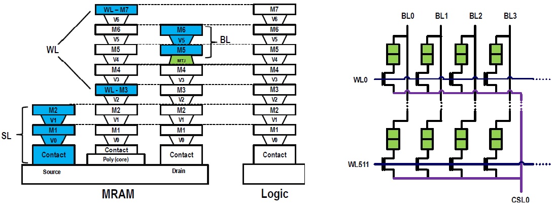
This STT-MRAM process offers a considerable cost advantage over scaling existing eFlash device technology.
In the image on the right above, the word lines run through the array connected to access devices. During a read cycle, the column select line is grounded, and the resistance of the active MTJ determines the bitline current. For a write cycle, since the MTJ programming current flows in opposite directions for a write to the AP state versus a write to the P state, the roles of the bitlines and column select lines are reversed, depending on the data value – i.e., write_1: BL = 0V, CS = VPP; write_0: BL = VPP, CS = 0V.
STT-MRAM technology does present some challenges, however.
- small read sensing window
The read cycle needs to sense the difference in MTJ resistance between parallel and anti-parallel states. Process variation in MTJ characteristics results in narrowing of this resistance contrast. Sophisticated sense amplifier design methods are needed to compensate for a tight resistance margin.
- strong MTJ sensitivity to temperature
The embedded MTJ IP will be subjected to temperature extremes both during assembly and during its operational lifetime. The solder ball reflow and package-to-PCB attach process temperature is far higher than the maximum operational temperature, albeit only once and for a relatively short duration. (Solder reflow temperatures are ~245C-260C.) The operational environment for the demanding nature of MCU applications typically spans -40C to 125C. The composition and diameter of the MTJ materials – i.e., the fixed and free magnetic layers, the tunneling oxide – are selected to maintain the spin-transfer torque properties throughout both assembly and operating temperature cycles.
Yet, due to the MTJ sensitivity to temperature, any attempt to pre-program data into the embedded STT-MRAM array prior to exposure to the assembly process temperatures would be fruitless. Special technology-design co-optimization (TDCO) methods are needed to initialize (a portion of) the STT-MRAM array with key data measured at wafer test – more on these methods shortly.
Also, the read sensitivity – i.e., the resistance difference of P and AP states – is reduced at high temperature. At cold temperature, the write current required to set the state of the bitcell is increased. Again, TDCO techniques are required to compensate for these reduced margins at different temperature extremes.
- process variation in MTJ characteristics
Sensing of the resistance differential also needs to address the process variation in MTJ devices, and the range of P and AP resistance states.
At the recent International Electron Devices Meeting (IEDM) conference in San Francisco, TSMC presented their TDCO approaches to address the STT-MRAM challenges above. [2] The rest of this article summarizes the highlights of their presentation, leading to the production release of STT-MRAM IP in their N22 ultra-low leakage process (N22ULL) node.
TSMC TDCO for N22ULL STT-MRAM
- read sensing
When an address word line is raised along a set of bitcells in the MRAM array, current flows through the MTJ from the (pre-charged) bitline to the (grounded) select line. The magnitude of the current on the bitline depends upon the P or AP state of the individual bitcell, and needs to be accurately sensed. The MTJ process variation across the array suggests that each bitline sense circuit must be individually “trimmed” to match the specific local characteristics of the devices. And, the strong temperature dependence of the MTJ needs to be dynamically compensated.
The optimized TSMC solution to MRAM bitline read sensing is illustrated below.
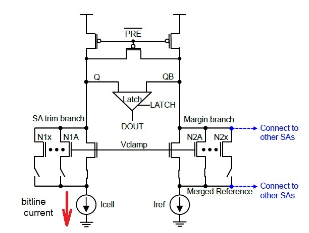
The read sense circuitry shown above is differential in nature, intended to amplify the voltage difference on lines Q and QB that evolves during the read cycle. Prior to the start of the read, both nodes Q and QB are pre-charged. When the address word line is raised, bitline current flows through the MTJ – in the figure above that is represented by current source Icell.
Note that the bitcells in the memory array are “single-ended” – i.e., there is only one connection to the sense amplifier. (This is in contrast to a conventional 6T SRAM bitcell, for example, which provides connections to both Q and QB of the sense amplifier.) As a result of the single connection, it is necessary to provide the QB line with a reference current, which needs to be between the Icell_P and Icell_AP values which may be flowing in the opposite side of the sense amplifier. Further, this reference current needs to adapt to the local die temperature.
TSMC developed a unique design approach to provide the Iref value to a set of N bitcells + sense amplifiers on a word line in the array.
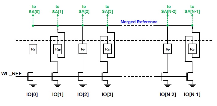
The figure above depicts N/2 reference MTJs that have been initialized to a P resistive state and N/2 reference MTJs in an AP state. Their outputs have been dotted to provide a “merged” reference current. The WL_REF signal is raised in a balanced timeframe as the active wordline – the resulting merged reference current is connected to the N sense amplifiers. As a result, the Iref current to an individual SA is:
((N/2) * I_P) + ((N/2) * I_AP) / N = (I_P + I_AP) / 2
or the ideal “midpoint” current on the QB line. After an appropriate duration into the read cycle, when a Q and QB voltage difference has been established, the Latch enable signal is raised to amplify the differential and drive Dout to the read value.
The approach to generate Iref for the sense amplifiers in an MRAM array bank provides both temperature compensation and some degree of “averaging” over process variation.
- sense amplifier trimming
Nevertheless, MTJ process variation necessitates a per-sense amplifier correct design technique. In the sense amplifier circuit figure above, devices N1A through N1X are in parallel with the sense pulldown transistor, all connected to Vclamp. The switches in series with these devices represent the capability to trim the resistance of the Q line during a read cycle. (The N2A through N2X devices provide a comparable, symmetric capability on the QB line, matching the loading on the Q line.) During wafer-level testing, the memory BIST macro IP includes programming support to adjust the “trim code” to realize the lowest number of bit read failures during BIST, with error-correction circuitry disabled. (This testing is performed at elevated temperature.)
- OTP-MRAM
It was mentioned earlier that the elevated temperatures to which the MTJ is subjected during assembly preclude any attempt to write data into the array during die test. Yet, the trim code values for each sense amplifier derived during memory BIST need to be retained in the array. (Also, any built-in array self-repair BISR codes identified after BIST testing need to be stored.)
To address this issue, TSMC developed a unique approach, where some of the MTJ cells are subjected to a one-time programming (OTP) write sequence. These cells retain their OTP values after exposure to the solder-reflow assembly temperature.
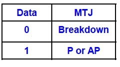
For these storage locations, a (tunnel oxide) “breakdown” voltage is applied to the MTJ to represent a stored ‘0’ value; the cell current will be high. As illustrated above, any OTP junction that does not receive an applied breakdown voltage during programming will remain (P or AP) resistive, and thus will be sensed as storing a fixed ‘1’ value.
- temperature-compensated write cycle
Whereas the sense amplifier (Rp versus Rap) read margin is reduced at high temperature, the MTJ write cycle is a greater challenge at low temps, where higher current are required to alter the MTJ state. TSMC developed an operational write-verify cycle, where the applied write voltage is dynamically adapted to temperature. The figure below shows a shmoo plot indicating the (wordline and bitline) write voltage sensitivity versus temperature (for AP-to-P and P-to-AP), and thus the need for compensation.
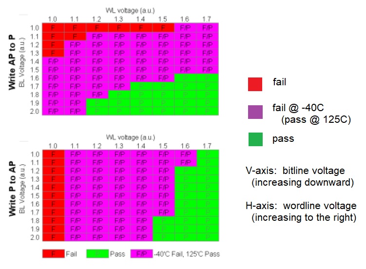
TSMC noted the “wakeup time” of the analog circuitry used to generate the corresponding write voltages adds minimally to the write cycle time.
Summary
At advanced process nodes, STT-MRAM IP offers an attractive evolution from eFlash for non-volatile storage – e.g., high retention, high durability, low additional process cost. TSMC recently presented their TDCO approach toward addressing the challenges of this technology, adopting several unique features:
- improved read sensing between Rp and Rap
- derivation of read sense amplifier reference current compensated for temperature, with process variation averaging
- per sense amplifier “trimming” for optimal read bit error rate
- one-time programming cell storage prior to solder reflow assembly, to retain trim codes and array repair values
- a temperature-compensated write voltage applied to the MTJ (as part of the write-verify cycle)
The characteristics and specs for the TSMC N22ULL STT-MRAM IP are appended below.
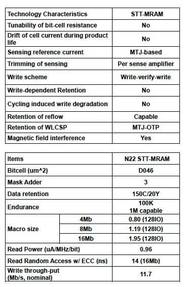
To quote TSMC, “Each emerging memory technology has its own unique advantages and challenges. Design innovation is essential to overcome the new challenges and bring the memory IP to market.”
-chipguy
References
[1] Shih, Yi-Chun, et al., “A Reflow-capable, Embedded 8Mb STT-MRAM Macro with 9nS Read Access Time in 16nm FinFET Logic CMOS Process”, IEDM 20, paper 11.4.
[2] Chih, Yu-Der, et al., “Design Challenges and Solutions of Emerging Nonvolatile Memory for Embedded Applications”, IEDM 2021, paper 2.4.
Note: All images are copyright of the IEEE.
Share this post via:


Comments
3 Replies to “Technology Design Co-Optimization for STT-MRAM”
You must register or log in to view/post comments.