Frequent SemiWiki readers are no doubt familiar with the advances in packaging technology introduced over the past decade. At the recent International Electron Devices Meeting (IEDM) in San Francisco, TSMC gave an insightful presentation sharing their vision for packaging roadmap goals and challenges, to address the growing demand for greater die integration, improved performance, and higher interconnect bandwidth.[1] This article summarizes the highlights of the presentation.
Background
2.5D packaging
2.5D packages enable multiple die to be laterally positioned in close proximity, with signal redistribution interconnect layers (RDL) between the die fabricated on a silicon interposer present between the die and package substrate. Through silicon vias (TSVs) provide the connectivity to the substrate.
The TSMC implementation of this technology is denoted as Chip-on-Wafer-on-Substrate (CoWoS), as was introduced a decade ago using multiple FPGA die in the package to expand the effective gate count.
The emergence of high bandwidth memory (HBM) stacked die as a constituent of the 2.5D integration offered system architects with new alternatives for the memory hierarchy and processor-to-memory bandwidth.
The development investment in 2.5D technology grew, now enabling the silicon interposer area to greatly exceed the “1X maximum” reticle size, to accommodate more (and more diverse) processing, memory and I/O die components (aka, “chiplets”).
Additional package fabrication steps incorporate local “trench capacitors” into the interposer. Oxide-poly-oxide-poly material layers fill the trench, with the poly connected to the RDL supply metal. The resulting decoupling capacitance reduces power supply droop considerably.
Alternative technologies have also been developed, replacing the full area silicon interposer with a local “silicon bridge” (CoWoS-L) between adjacent die embedded in an organic interposer, thus reducing cost (albeit with relaxed RDL interconnect dimensions).
Concurrently, for very low cost applications, the demand for higher I/O count die than could be supported with the conventional wafer-level chip-scale package (WLCSP) led to the development of a novel technology that expands the die surface area with a “reconstituted wafer”, on which the redistribution to a larger number of I/O bumps could be fabricated.
This Integrated FanOut (InFO) technology was originally developed for single die (as a WLCSP-like offering). Yet, the application of this technique is readily extended to support the 2.5D integration of multiple heterogeneous die placed adjacent, prior to the reconstitution step. (The InFO_oS technology will be discussed shortly.)
3D die stacking
3D die stacking technology has also evolved rapidly. As mentioned above, the fabrication of TSVs spanning between layers of DRAM memory die with “microbumps” attached at the other end of the TSV has enabled impressive levels of vertical stacking – e.g., eight memory die plus a base logic controller die in an HBM2e configuration.
Similarly, through-InFO vias (located outside the base die in the reconstituted wafer material) has enabled additional micro-bumped die to be vertically stacked above the base InFO die – e.g., a memory die on top of a logic die.
The most recent advancement in 3D stacking technology has been to employ bump-less “direct bonding” between two die surfaces. Applying a unique thermal + compression process, two die surfaces are joined. The metal pad areas on the different die expand to form an electrical connection, while the abutting dielectric surfaces on the two die are bonded. Both face-to-face (F2F) and face-to-back (F2B) die orientations are supported. The planarity and uniformity (warpage) requirements of the surfaces are demanding; particulates present on the surface are especially problematic. TSMC denotes their 3D package technology as System-on-Integrated Chips, or “SoIC”.
As product architects are exploring the opportunities available with these packaging technologies, there is growing interest in combining “front-end” 3D stacked SoIC configurations with 2.5D “back-end” (InFO or CoWoS) RDL patterning and assembly. The collective brand that TSMC has given to their entire suite of advanced packaging offerings is “3D Fabric”, as illustrated below.
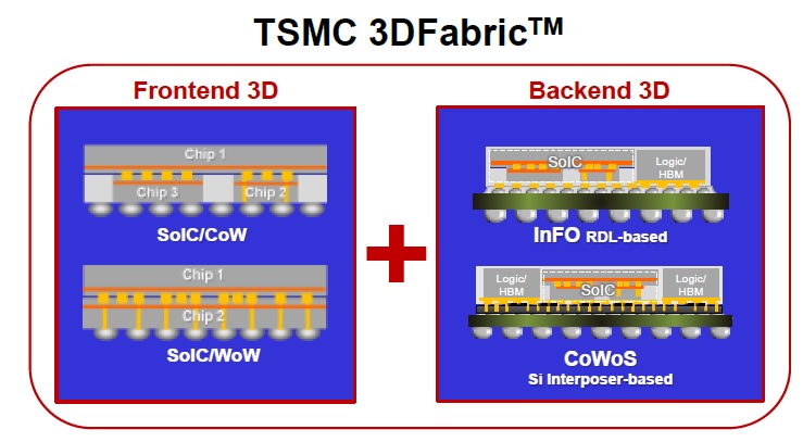
TSMC 3D Fabric Roadmap
At IEDM, TSMC shared their strategy for improving performance, power efficiency, signal bandwidth, and heat dissipation for these technologies. (The majority of the focus was on bonding technology for SoIC.)
CoWoS (2.5D)
-
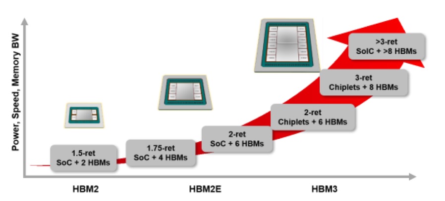
- increase package dimensions to 3X maximum reticle size for the Si interposer
- expectation is that stacked SoIC die will be integrated with multiple HBM stacks
InFO_oS (2.5D)
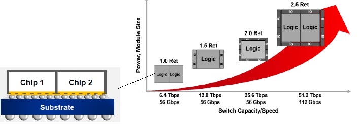
The original InFO offering was as an evolution to WLCSP, first as a single die, and then as a base die with another added on top connected to the through-InFO vias. TSMC is also expanding the InFO offering to support multiple adjacent die embedded in the reconstituted wafer; the RDL layers are then fabricated and microbumps added for attach to a substrate (InFO-on-Substrate, of InFO_oS). A projection for the InFO_oS configurations to be supported is illustrated below.
SoIC (3D)
The roadmap for 3D package development is shown below, followed by a table illustrating the key technical focus – i.e., scaling the bond pitch of the (F2F or F2B) stacked connections.
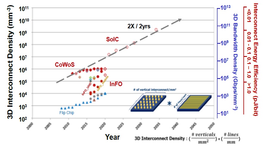
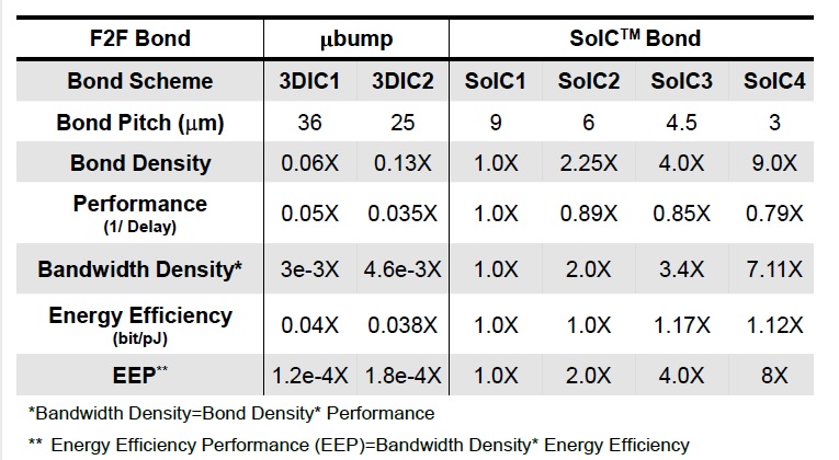
The bond pitch (and other metrics) for microbump technology evolution are included with the SoIC direct bonding measures in the table above for comparison.
As shown in the table above, TSMC has defined a new (relative comparison) metric to represent the roadmap for 3D stack bonding technology – an “Energy Efficiency Performance” (EEP) calculation. Note that the target gains in EEP are driven by the aggressive targets for scaling of the bond pitch.
EEP = (bond_density) * (performance) * (energy efficiency)
Much like the IC scaling associated with Moore’s Law, there are tradeoffs in 3D bond scaling for performance versus interconnect density. And, like Moore’s Law, the TSMC roadmap goals are striving for a 2X improvement in EEP for each generation.
SoIC Futures
As an illustration of the future potential for 3D stacking, TSMC provided an example of a three-high stacked structure, as shown below.
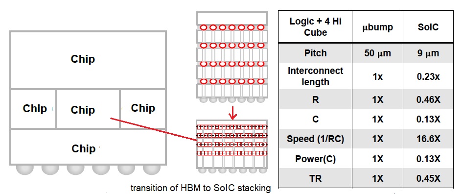
Note that the assumption is that future HBM stacks will migrate from a microbump attach technology within the stack to a bonded connection – the benefits of this transition on performance, power, and thermal resistance (TR) are also shown in the figure.
heat dissipation
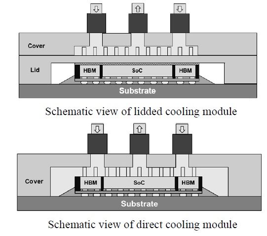
Speaking of thermal resistance, TSMC emphasized the importance of both the bonding process for low TR and design analysis of the proposed 3D stack configuration, to ensure the junction temperature (Tj) across all die remains within limits.
The IEDM presentation referred to additional research underway at TSMC to evaluate liquid-cooling technology options. [2] As illustrated below, “micro-pillars” can be etched into a silicon lid bonded to the assembly, or even directly into the die, for water cooling.
Summary
Advanced 2.5D and 3D packaging technologies will provide unique opportunities for systems designers to optimize performance, power, form factor (area and volume), thermal dissipation, and cost. TSMC shared their development roadmap for both 2.5D and 3D configurations.
The 2.5D focus will remain on support of larger substrate sizes for more (heterogeneous) die integration; for markets focus on cost versus performance, different interposer/bridge (CoWoS) and reconstituted wafer (InFO technology options are available.
3D stacking technology will receive the greatest development focus, with an emphasis on scaling the interface bond pitch. The resulting “2X improvement in EEP” for each SoIC generation is the target for the new “More than Moore” semiconductor roadmap.
-chipguy
References
[1] Yu, Douglas C.H., et al, “Foundry Perspectives on 2.5D/3D Integration and Roadmap”, IEDM 2021, paper 3-7.
[2] Hung, Jeng-Nan, et al., “Advanced System Integration for High Performance Computing with Liquid Cooling”, 2021 IEEE 71st Electronic Components and Technology Conference (ECTC), p. 105-111.
Note: All images are copyright of the IEEE.
Share this post via:


Comments
One Reply to “Advanced 2.5D/3D Packaging Roadmap”
You must register or log in to view/post comments.