Back in April, 2019, TSMC announced that they were introducing their 5 nm technology in risk production and now at IEDM 2019 they brought forth a detailed description of the process which has passed 1000 hour HTOL and will be in high volume production in 1H 2020. This 5nm technology is a full node scaling from 7nm using smart scaling of major design rules (gate, fin and Mx/Vx pitches) for improved yield featuring an SRAM cell of 0.021um2 and a declining defect density D0 that is ahead of plan.
A primary reason for the success of the 5nm technology platform is the implementation of Extreme Ultra-Violet (EUV) photolithography. Fully-fledged EUV replaces at least four times more immersion layers at cut, contact, via and metal line masking steps for faster cycle time, better reliability and yield. Total mask count in 5nm is several masks less than in the previous 7nm node. Fig. 1 shows how one EUV mask replaced five immersion masks yet produces better patterning fidelity, shorter cycle time and fewer defects.
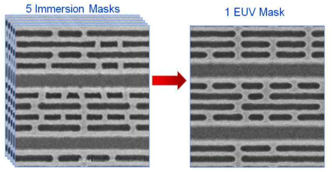
Fig. 1. Diagram of BEOL metallization comparing EUV vs. immersion photolithography showing how one EUV mask replaced five immersion patterning layers with better patterning fidelity, shorter cycle time and fewer defects.
FinFETs have been used in four generations from the 16nm node to 7nm, but performance as a function of channel mobility has been stagnant. To address this, the High Mobility Channel (HMC) was implemented to increase performance. The TEM in Fig. 2 shows the fully-strained HMC lattice constant interfaced with the Si lattice constant. The diffraction pattern confirmed HMC strain.
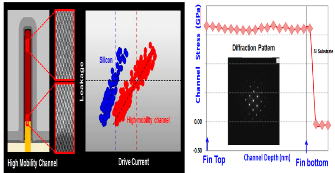
Fig. 2. Diagram showing finFET cross-section TEM showing fully-strained HMC lattice constant interfaced with the Si lattice constant. The second plot shows higher leakage vs drive current of the silicon vs HMC transistors. The third plot shows the channel stress in GPa vs channel depth from the fin top to the fin bottom. The diffraction pattern shown confirms the HMC strain.
The HMC finFET has excellent Id-Vg characteristics as shown in Fig. 3 and produces ~18% more drive current than the Si finFET. Figure-of-Merit (FOM) ring oscillator standby power also correlates well to transistor leakages.
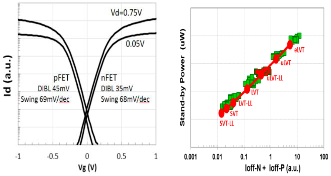
Fig. 3. Chart showing drain current vs gate voltage (Id vs Vg) characteristics of the High Mobility Channel (HMC) transistors for different drain voltages. The second plot shows the off-current ranges, Ioff-N and Ioff-P and the relative impact on standby current of the seven different Vt’s available in the technology. The currents in both diagrams are in logarithmic scale with one decade per division. The Drain-Induced Barrier Lowering (DIBL) is 45mV and 35 mV and the swing is 69mV and 68mV for p-channel and n-channel transistors respectively.
This 5nm CMOS platform technology is a full node scaling from the 7nm process described in IEDM 2016. The availability of up to seven Vt’s for each transistor type, shown in Fig. 4, enables product design to meet the needs of power efficiency in mobile SoC as well as peak speed requirements of HPC.
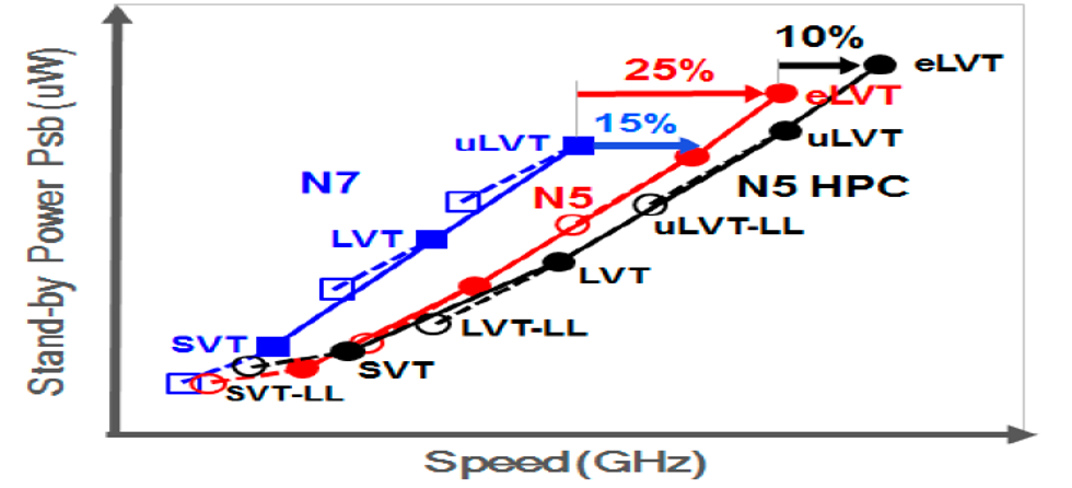
Fig. 4. Chart of up to seven Vt’s available in N5 showing standby power in uW vs speed in GHz for N5 and N5 HPC compared to N7 to meet maximum power efficiency for mobile and peak speed in HPC. eLVT offers 25% faster peak speed over 7nm. Silicon data close to matching FOM ring speed vs stand-by power.
New HPC features are the extremely Low VT (eLVT) transistor with 25% faster peak speed over 7nm and three-fin standard cells for an additional 10% performance increase. The technology is available for 3D chip stacking using hybrid bonding. In addition to impressive density and performance gains relative to 7nm, the technology has achieved 1000 hour HTOL qualification with improved stress aging characteristics relative to the 7nm technology. The high-yielding SRAM and logic defect density D0 is ahead of plan. Technological achievements enabling this progress feature full-fledged implementation of EUV and high-mobility channel (HMC) finFETs.
This 5nm platform technology was designed and developed to meet objectives of PPACT(Power, Performance, Area, Cost and Time to Market). Design-Technology Co-Optimization (DTCO) is emphasized for smart scaling, avoiding brute-force scaling which would lead to drastically-increased process cost and yield impact. Design features such as gate-contact-over-diffusion and unique diffusion termination along with EUV-based gate patterning enable SRAM size reduction and increased logic density. The 5nm technology offers 15% faster speed at the same power or 30% power reduction at the same speed with 1.84x logic density of the 7nm node , as shown in Fig. 5.
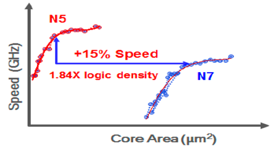
Fig. 5. Plot comparing the speed in GHz vs. the core area in um2 of the N5 technology vs the previous N7. The 5nm technology offers 15% faster speed at the same power or 30% power reduction at the same speed with 1.84x logic density of the 7nm node.
Interconnect delay has a critical impact on product performance and with each generation the interconnect propagation delay has been getting significantly worse. Backend metal RC and via resistance is shown in Fig. 6 for generations from N28 to N5. The tightest pitch Mx RC and the Vx Rc are kept similar to the 7nm node by EUV patterning, innovative scaled barrier/liner ESL/ELK dielectrics and Cu reflow.
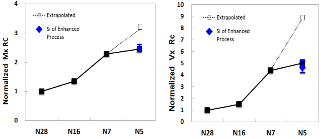
Fig. 6. Charts of normalized BEOL metallization RC product and via resistance vs nodes from N28 to N5 are shown. For the tightest metal pitch, MX RC and via resistance Vx Rc are kept similar to that of the previous 7nm node by EUV patterning, innovative scaled barrier/liner ESL/ELK dielectrics and Cu reflow.
SRAM density and performance/leakage are critical for mobile SoC and for HPC AI. Scaling of SRAM cells with more advanced nodes is becoming more difficult in feature size terms of F 2. The offered High Current (HC) and the High Density (HD) SRAM cells with cell areas of 0.025um2 and 0.021 um2 respectively are the densest in the industry as shown in Fig. 7. Consistent high yield of the 256 Mb SRAM and logic test chips of >90% peak yield and ~80% average yield (without repair) has been achieved.
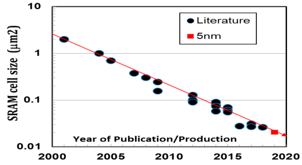
Fig. 7. Chart of published SRAM cell size in um2 vs year of publication. The 5nm HD SRAM cell at 0.021 um2 is the densest offered in the industry.
The Ultra-low leakage ULHD can be used to reduce retention leakage for better power efficiency while higher-speed HSHD SRAM may be used as an alternative to HC SRAM cells to allow ~22% reduction in memory area as shown in Fig. 8.
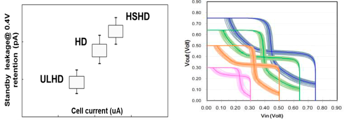
Fig. 8. Chart of standby leakage in pA at 0.4V vs cell current in uA for ULHD, HSHD and standard HD SRAM cells. The Vout vs Vin butterfly curve plots of the 5nm HD SRAM cell are shown at voltages from 0.75V down to 0.3V.
The shmoo plot of the 256Mb 0.021 um2 HD SRAM cell with full read/write function is shown down to 0.4V in Fig. 9.
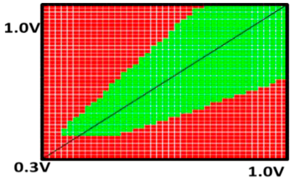
Fig. 9. Shmoo plot showing Vout vs Vin from 1.0V down to 0.4V of the 256Mb SRAM based on the 5nm 0.021 um2 HD SRAM cell.
The frequency response shmoo plots of the GPU and CPU blocks in the high-yielding logic test chip are shown in Fig. 10.
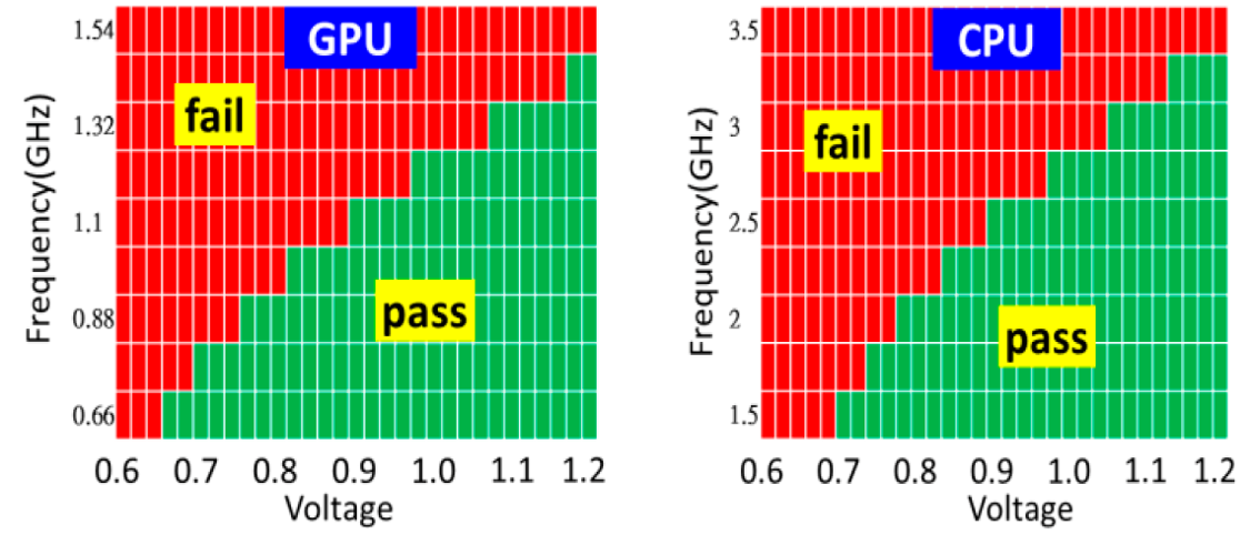
Fig. 10. Shmoo plots of frequency in GHz vs. voltage for the GPU and CPU blocks respectively in the high yielding logic test chip in the 5nm qualification vehicle.
The 256Mb HD/HC SRAM and logic test chip passed 1000 hour HTOL qualification. The SRAM Vmin showed a negligible shift at 168 hours and passed the 1000 hour HTOL with ~51mV margin as shown in Fig. 11.
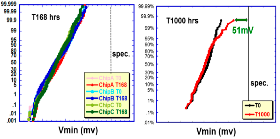
Fit. 11. Plots of log-normal distribution vs Vmin in mV at 168 hours HTOL showing negligible Vmin shift and at 1000 hours HTOL, passing 1000 hours with 51mV margin.
Stress aging data at 0.96 V and 125C on the 5nm FOM ring oscillator made with the High Mobility Channel finFETs shown in Fig. 12 with improved aging relative to the 7nm node.
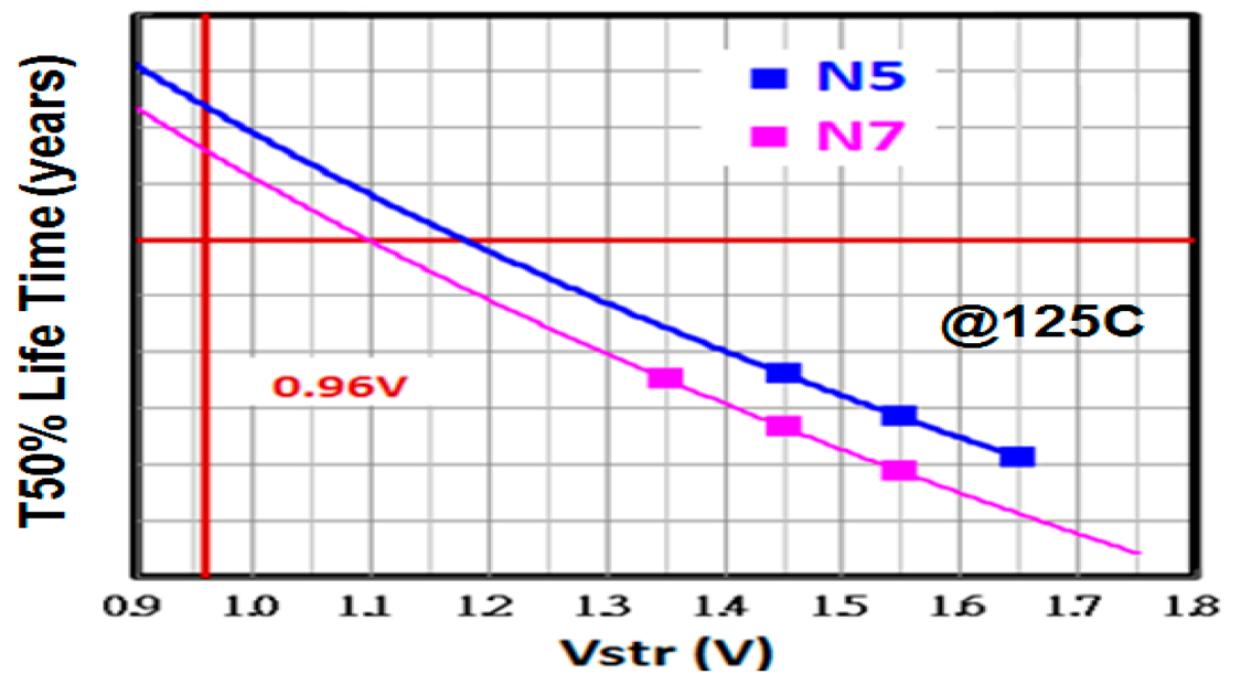
Fig. 12. Plot showing T50% lifetime(years) vs. stress voltage Vstr of aging study at 125C of N5 HMC finFET ring oscillators and N7 silicon finFET ring oscillators showing improved aging at the 5nm node relative to that at 7nm.
Another important feature for HPC is the metal-insulator-metal (MiM) capacitor formed in the upper layers of the BEOL metallization. The 5nm node MiM has 4x higher capacitance density than the typical HD-MiM and produces ~4.2% faster Fmax by minimizing transient drooping voltage and achieved ~20mV Vmin reduction in a CPU test chip.
HPC critically depends on high-speed IOs especially SERDES. By successfully optimizing finFET driving strength and capacitance/resistance with special high-speed devices, PAM-4 SERDES transmitter speed of 112 Gb/s at 0.78 pJ/bit and 130 Gb/s at 0.96pJ/b power dissipation as shown in Fig. 13.
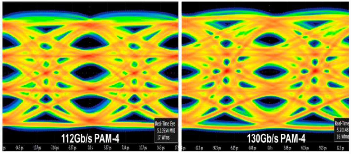
Fig. 13. Plots showing signal characteristics of voltage out in mV vs time in ps of 112 Gb/s and 130Gb/s data transmission in SERDES PAM-4 with 0.78pJ/b and 0.96pJ/b respectively.
In conclusion, TSMC has presented a very competitive technology platform, establishing itself as the leader in best-in-class highest density logic technologies. Volume production in 1H 2020 will enable leading edge products in advanced SoC for mobile, especially 5G, as well as HPC applications for AI, datacenter and blockchain products which increasingly need high performance with best power efficiency.
Share this post via:


Comments
18 Replies to “TSMC Unveils Details of 5nm CMOS Production Technology Platform Featuring EUV and High Mobility Channel FinFETs at IEDM2019”
You must register or log in to view/post comments.