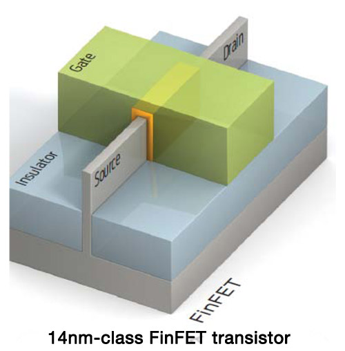
 The common theme amongst semiconductor ecosystem conferences this year is FinFETS, probably the most exciting technology we will see this decade. A lot has been written on SemiWiki about FinFETS, it is one of the top trending search terms, but there is some confusion about the process naming so let me attempt to explain.
In planar process technologies the 28nm or 20nm implies the minimum transistor gate length of 28nm or 20nm. Corresponding to that lithographic capability are two other critical dimensions: the “contacted gate pitch” and the “metal pitch” for the lowest, thinnest metal layers. (Higher metal layers will be thicker with less resistance which are more suitable for longer routes but will have a greater width+space design pitch.)
Given that, the 16nm FinFET process technology is a bit of a misnomer. It was probably named by Marketing people to imply that the resulting performance when transitioning from planar to FinFET in a 20nm lithography process would be “between 20nm planar and 14nm FinFET”.
Why 16nm FinFETS you ask? Two reasons: (1) EUV is late so a true 14nm FinFET process will not be possible by 2015 and (2) Customers designing mobile devices were not willing to wait for the power savings FinFETS have to offer. As a result, the current 20nm lithography process was modified for FinFETs, and the 16nm FinFET process was born.
If you were to ask, “What is the minimum gate length, contacted gate pitch and metal pitch for 16nm FF, and how does that differ from 20nm SoC?”, you would get the answer that it’s the same litho design rules, just a different transistor structure.
There is one additional measurement that is introduced in a FinFET technology: the effective device width per micron. These are transistor parameters, and they are an indicator of performance, but they are relatively independent of the contacted gate pitch + metal pitch, which define the achievable circuit density.
The IBM 14nm FinFET tape out briefing provided some interesting process details. Disclosing this type of information is certainly not IBM-like so the stakes are obviously high in the race to FinFETs:
[TABLE] align=”left” style=”width: 470px”
|-
|
| 32nm
| 28nm
| 20nm
| 14nm
|-
| Architecture
| Planar
| Planar
| Planar
| FinFET
|-
| Contacted poly pitch
| 126nm
| 114nm
| 90nm
| 80nm
|-
| Metal pitch
| 100nm
| 90nm
| 64nm
| 64nm
|-
| Local interconnect
| No
| No
| Yes
| Yes
|-
| Self-aligned contact
| No
| No
| No
| No
|-
| Strain engineering
| Yes
| Yes
| Yes
| Yes
|-
| Double patterning
| No
| No
| Yes
| Yes
|-
Bottom line, lithographically, both 16nm and 14nm FinFET processes are still effectively offering a 20nm technology with double-patterning of lower-level metals and no triple or quad patterning.
One team has chosen to define the performance of their FinFET as a “half node” improvement (e.g., 20nm ->16nm), whereas the other has chosen to represent the performance of their FinFET as equivalent to a “full-node shrink” (20nm -> 14nm). There will be slightly different fin_height, fin_thickness, and fin_pitch parameters between the two processes but the circuit density is really still the same as 20nm.
Some designs might be smaller but in general I think FinFets at 16nm and 14nm will offer significantly lower power consumption and leakage but only marginally better performance and area than 20nm planar, just my opinion of course.
Who do you think will be first to get FinFETS into volume production? Would it be TSMC, Samsung, or GF? Check out the SemiWiki FinFET poll HERE. Anybody can vote so please do.
Also see:
Share this post via:


Comments
0 Replies to “16nm FinFET versus 20nm Planar!”
You must register or log in to view/post comments.