Today TSMC announced three reference flows that they have been working on along with various EDA vendors (and ARM and perhaps other IP suppliers). The three new flows are:
- 16FinFET Digital Reference Flow. Obviously this has full support for non-planar FinFET transistors including extraction, quantized pitch placement, low-vdd operation, electromigration and power management.
- 16FinFET Custom Design Reference Flow. This supports the non-digital stuff. It allows full customer transistor level design and verification including analog, mixed-signal, custom digital and memory.
- 3D IC Reference Flow, addressing vertical integration with true 3D stacking using both TSV through active silicon and/or using interposers.
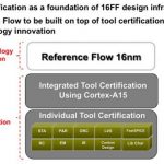
There have been multiple silicon test vehicles. The digital reference flow uses an ARM Cortex-A15 multicore processor as a validation vehicle and helps designers understand the challenges of full 3D RC modeling and quantized transistor widths, which are the big “new” gotchas in the FinFET world. The flow also includes methodology and tools for improving PPA in 16nm including low voltage operation analysis, high resistance layer routing optimization, path based analysis and graph based analysis correlation to improve timing closure.
By definition there is less automation in the custom reference flow because it’s custom and the designer is expected to do more by hand. But obviously it includes the verification necessary for compliance with 16nm manufacturing and reliability requirements.
The 3D IC flow allows everything to move up into the third dimension. This is still work in progress so I don’t think this will be any type of final 3D flow. But it supports what you would expect: the capability to stack die using through-transistor-stacking (TTS), through-silicon-vias & microbumps, backside metal routing, TSV to TSV coupling extraction.
So what is TTS? It is TSMC’s own name for TSV on wafers containing active devices (as opposed to on interposers, which typically only contain metal routing and decaps, where they still use the TSV name). The 3D test vehicle has stacked memories on top of 28nm SoC logic die (connected via microbumps). The 28nm logic die has TSVs through active silicon and connects to the backside routing (also called re-distribution layer or RDL) and C4 bumps on the backside of the logic die. The bumps then connect to standard substrate on the module. So this is true 3D, not 2.5D where die are bumped and flipped onto an interposer, and only the interposer (which doesn’t contain active devices) has TSVs. One of the challenges of TSVs is that the stress of manufacturing them alters transistor threshold voltages in the vicinity, and probably other stuff I’ve not heard about.
So FinFETs are coming at 16nm and the flows are ready to start designs, already validated in silicon. Plus a true 3D More than Moore flow.
OIP is coming up on October 1st. I’m sure that one of the keynotes will have some more about 16nm and 3D. For details and to register go here.