2019 TSMC Technology Symposium Review Part I

2019 TSMC Technology Symposium Review Part I
by Tom Dillinger on 04-30-2019 at 7:00 am

Each year, TSMC conducts two major customer events worldwide – the TSMC Technology Symposium in the Spring and the TSMC Open Innovation Platform Ecosystem Forum in the Fall. The Technology Symposium event was recently held in Santa Clara, CA, providing an extensive update on the status of advanced semiconductor and packaging technology development. This article briefly reviews the highlights of the semiconductor process presentations – a subsequent article will review the advanced packaging announcements.

First, some general items that might be of interest:

Longevity
TSMC was founded in 1987, and has been holding annual Technology Symposium events since 1994 – this was the 25th anniversary (which was highlighted prevalently throughout the Santa Clara Convention Center). “The first Silicon Valley symposium had less than 100 attendees – now, the attendance exceeds 2000.”, according to Dave Keller, President and CEO of TSMC North America.

Best Quote of the Day
Dr. Cheng-Ming Lin, Director, Automotive Business Development, describes the unique requirements of TSMC’s automotive customers, specifically with regards to continuity of supply over a much longer product lifetime. He indicated,

“Our commitment to legacy processes is unwavering. We have never closed a fab or shut down a process technology.” (Wow.)

Best Quip of the Day
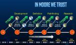
Dr. Y.-J. Mii, Senior Vice President of Research and Development / Technology Development , highlighted three eras of process technology development, as depicted in the figure below from his presentation.

In the first phase, Dennard scaling refers to the goal of scaling FEOL linear lithographic dimensions by a factor of “s” (s < 1) in successive process nodes, achieving an improvement of (1 / s**2) in circuit density, measured as gates / mm**2. The next phase focused on material improvements, and the current phase centers on design-technology co-optimization – more on that shortly.

In a subsequent presentation at the symposium, Dr. Doug Yu, VP, Integrated Interconnect and Packaging R&D, described how advanced packaging technology has also been focused on scaling, albeit for a shorter duration. “For over 10 years, packages have also offered two-dimensional improvements to redistribution layer (RDL) and bump pitch lithography. With the multi-die, 3D vertical stacking package technology we’re describing today – specifically, TSMC’s SoIC offering – we are providing vast improvements in circuit density. S is equal to zero. Or, in other words, infinite scaling. 😀 (Indeed, it is easy to foresee product technologies starting to use the metric “gates / mm**3” .)

Here is a brief recap of the TSMC advanced process technology status.

N7/N7+
TSMC announced the N7 and N7+ process nodes at the symposium two years ago. (link)

N7 is the “baseline” FinFET process, whereas N7+ offers improved circuit density with the introduction of EUV lithography for selected FEOL layers. The transition of design IP from N7 to N7+ necessitates re-implementation, to achieve a 1.2X logic gate density improvement. Key highlights include:


  • N7 is in production, with over 100 new tapeouts (NTOs) expected in 2019
  • Key IP introduction: 112Gbps PAM4 SerDes
  • N7+ is benefitting from improvements in sustained EUV output power (~280W) and uptime (~85%). “Although we anticipate further improvements in power and uptime, these measures are sufficient to proceed to N7+ volume ramp.”, TSMC said.
  • TSMC has focused on defect density (D0) reduction for N7. “The D0 improvement ramp has been faster than previous nodes, at a comparable interval after initial production volume ramp.”, according to TSMC.
  • TSMC illustrated a dichotomy in N7 die sizes – mobile customers at <100 mm**2, and HPC customers at >300 mm**2.
  • To my recollection, for the first time TSMC also indicated they are tracking D0 specifically for “large chips”, and reported a comparable reduction learning for large designs as for other N7 products.
  • N7+ will enter volume ramp in 2H2019, and is demonstrating comparable D0 defect rates as N7.

“Making 5G a Reality”
TSMC invited Jim Thompson, CTO, Qualcomm, to provide his perspective on N7 – a very enlightening presentation:

  • “N7 is the enabler for the 5G launch, as demonstrated in our latest Snapdragon 855 release.”
  • “5G MIMO with 256 antenna elements supports 64 simultaneous digital streams – that’s 16 users each receiving 4 data streams to a single phone.”
  • “Antenna design is indeed extremely crucial for 5G, to overcome path loss and signal blockage. There are new, innovative antenna implementations being pursued – in the end, it’s just math, although complex math for sure.”
  • “There’s certainly lots of skepticism about the adoption rate of 5G. Yet 5G is moving much faster than 4G did – at a comparable point in the rollout schedule, there were only 5 operators and 3 OEM devices supporting 4G, mostly in the US and South Korea. Currently, there are over 20 operators and over 20 OEM devices focused on 5G deployment, including Europe, China, Japan, and Southeast Asia.”
  • “And, don’t overlook the deployment of 5G in applications other than consumer phones, such as ‘wireless factory automation’. Communication to/from industrial robots requires high bandwidth, low latency, and extremely high availability. Consider the opportunities for manufacturing flexibility in a wire-free environment, enabled by 5G.”

N6
TSMC introduced a new node offering, denoted as N6. This node has some very unique characteristics:

  • design rule compatible with N7 (e.g., 57mm M1 pitch, same as N7)
  • IP models compatible with N7
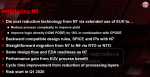
  • incorporates EUV lithography for limited FEOL layers – “1 more EUV layer than N7+, leveraging the learning from both N7+ and N5”
  • tighter process control, faster cycle time than N7
  • same EDA reference flows, fill algorithms, etc. as N7
  • N7 designs could simply “re-tapeout” (RTO) to N6 for improved yield with EUV mask lithography
  • or, N7 designs could submit a new tapeout (NTO) by re-implementing logic blocks using an N6 standard cell library (H240) that leverages a “common PODE” (CPODE) device between cells for an ~18% improvement in logic block density
  • risk production in 1Q’20 (a 13 level metal interconnect stack was illustrated)
  • although design rule compatible with N7, N6 also introduces a very unique feature – “M0 routing”

The figure below illustrates a “typical” FinFET device layout, with M0 solely used as a local interconnect, to connect the source or drain nodes of a multi-fin device and used within the cell to connect common nFET and pFET schematic nodes.


I need to ponder a bit more on the opportunity use M0 as a routing layer – TSMC indicated that EDA router support for this feature is still being qualified.

N6 strikes me as a continuation of TSMC’s introduction of a “half node” process roadmap, as depicted below.


A half-node process is both an engineering-driven and business-driven decision to provide a low-risk design migration path, to offer a cost-reduced option to an existing N7 design as a “mid-life kicker”.

The introduction of N6 also highlights an issue that will become increasingly problematic. The migration of a design integrating external IP is dependent upon the engineering and financial resources of the IP provider to develop, release (on a testsite shuttle), characterize, and qualify the IP on a new node on a suitable schedule. N6 offers an opportunity to introduce a kicker without that external IP release constraint.

N5
The process node N5 incorporates additional EUV lithography, to reduce the mask count for layers that would otherwise require extensive multipatterning.


  • risk production started in March’19, high volume ramp in 2Q’20 at the recently completed Gigafab 18 in Tainan (phase 1 equipment installation completed in March’19)
  • intended to support both mobile and high-performance computing “platform” customers; high-performance applications will want to utilize a new “extra low Vt”(ELVT) device
  • 1.5V or 1.2V I/O device support
  • an N5P (“plus”) offering is planned, with a +7% performance boost at constant power, or ~15% power reduction at constant perf over N5 (one year after N5)
  • N5 will utilize a high-mobility (Ge) device channel

Advanced Materials Engineering
In addition to the N5 introduction of a high mobility channel, TSMC highlighted additional materials and device engineering updates:

  • super high-density MIM offering (N5), with 2X ff/um**2 and 2X insertion density
  • new low-K dielectric materials
  • metal Reactive Ion Etching (RIE), replacing Cu damascene for metal pitch < 30um
  • a graphene “cap” to reduce Cu interconnect resistivity

An improved local MIM capacitance will help to address the increased current from the higher gate density. TSMC indicated an expected single-digit % performance increase could be realized for high-performance (high switching activity) designs.

Nodes 16FFC and 12FFC both received device engineering improvements:

  • 16FFC+ : +10% perf @ constant power, +20% power @ constant perf over 16FFC
  • 12FFC+ : +7% perf @ constant power, +15% power @ constant perf over 12FFC

NTO’s for these nodes will be accepted in 3Q’19.

TSMC also briefly highlighted ongoing R&D activities in materials research for future nodes – e.g., Ge nanowire/nanoslab device channels, 2D semiconductor materials (ZrSe2, MoSe2) – see the figure below (Source: TSMC).

Manufacturing Excellence
Dr. J.K. Wang, SVP, Fab Operations, provided a detailed discussion of the ongoing efforts to reduce DPPM and sustain “manufacturing excellence”. Of specific note were the steps taken to address the demanding reliability requirements of automotive customers. Highlights of Dr. Wang’s presentation included:

“Since the introduction of the N16 node, we have accelerated the manufacturing capacity ramp for each node in the first 6 months at an ever-increasing rate. The N7 capacity in 2019 will exceed 1M 12” wafers per year. The N10/N7 capacity ramp has tripled since 2017, as phases 5 through 7 of Gigafab 15 have come online.”

“We have implemented aggressive statistical process control (measured on control wafer sites) for early detection, stop, and fix of process variations – e.g., upward/downward shifts in baseline measures, a variance shift, mismatch among tools. We have established 2D wafer profile measurement criteria, and in-line monitoring and comparison to an “acceptance” profile across each wafer.”

“The DDM reduction rate on N7 has been the fastest of any node.”

“For automotive customers, we have implemented unique measures to achieve the demanding DPPM requirements. We will ink out good die in a bad zone. And, there are SPC criteria for a maverick lot, which will be scrapped.”

“We will support product-specific upper spec limit and lower spec limit criteria. We will either scrap an out-of-spec limit wafer, or hold the entire lot for the customer’s risk assessment.”
(See the figures below. Source: TSMC)


Automotive Platform

TSMC has developed an approach toward process development and design enablement features focused on four platforms – mobile, HPC, IoT, and automotive. Dr. Cheng-Ming Lin, Director, Automotive Business Unit, provided an update on the platform, and the unique characteristics of automotive customers.

Growth in semi content
Dr. Lin indicated, “Automotive systems will require both advanced logic technologies for ADAS, such as N16FFC, and advanced RF technologies for V2X communications. Although the CAGR for cars from now to 2022 is expected to be only ~1.8%, the CAGR for the semiconductor content will be 6.9%.”

He continued, “The L1/L2 feature adoption will reach ~30%, with additional MCU’s applied to safety, connectivity, and EV/hybrid EV features. There will be ~30-40 MCU’s per vehicle. “ (In his charts, the forecast for L3/L4/L5 adoption is ~0.3% in 2020, and 2.5% in 2025.)

“The adoption rate for the digital dashboard cockpit visualization system will also increase, driving further semiconductor growth – 0.2% in 2018 to 11% in 2025.”

L2+
The levels of support for automated driver assistance and ultimately autonomous driving have been defined by SAE International as “Level 1 through Level 5”. Perhaps in recognition of the difficulties in achieving L3 through L5, a new “L2+” level has been proposed (albeit outside of SAE), with additional camera and decision support features.

“An L2+ car would typically integrate 6 cameras, 4 short-range radar systems, and 1 long-range radar unit, requiring in excess of 50GFLOPS graphics processing and >10K DMIPS navigational processing throughput.”

N16FFC, and then N7
The 16FFC platform has been qualified for automotive environment applications – e.g., SPICE and aging models, foundation IP characterization, non-volatile memory, interface IP. The N7 platform will be (AEC-Q100 and ASIL-B) qualified in 2020. “Automotive customers tend to lag consumer adoption by ~2-3 years, to leverage DPPM learning – although that interval is diminishing. We anticipate aggressive N7 automotive adoption in 2021.”,Dr. Lin indicated.

“The TSMC RF CMOS offerings will be used for SRR, LRR, and Lidar. The 16FFC-RF-Enhanced process will be qualified for automotive platforms in 2Q’20.”

IoT Platform
The TSMC IoT platform is laser-focused on low-cost, low (active) power dissipation, and low leakage (standby) power dissipation. Dr. Simon Wang, Director, IoT Business Development, provided the following update:

Process Roadmap

  • 55ULP, 40ULP (w/RRAM): 0.75V/0.7V
  • 22ULP, 22ULL: 0.6V
  • 12FFC+_ULL: 0.5V (target)
  • introduction of new devices for the 22ULL node: EHVT device, ultra-low leakage SRAM

The 22ULL SRAM is a “dual VDD rail” design, with separate logic (0.6V, SVT + HVT) and bitcell VDD_min (0.8V) values for optimum standby power.

The 22ULL node also get an MRAM option for non-volatile memory.

Note that a new methodology will be applied for static timing analysis for low VDD design. The stage-based OCV (derating multiplier) cell delay calculation will transition to sign-off using the Liberty Variation Format (LVF).

The next generation IoT node will be 12FFC+_ULL, with risk production in 2Q’20. (with low VDD standard cells at SVT, 0.5V VDD).

RF
TSMC emphasized the process development focus for RF technologies, as part of the growth in both 5G and automotive applications. Dr. Jay Sun, Director, RF and Analog Business Development provided the following highlights:

  • For RF system transceivers, 22ULP/ULL-RF is the mainstream node. For higher-end applications, 16FFC-RF is appropriate, followed by N7-RF in 2H’20.
  • Significant device R&D is being made to enhance the device ft and fmax for these nodes – look for 16FFC-RF-Enhanced in 2020 (fmax > 380GHz) and N7-RF-Enhanced in 2021.
  • New top-level BEOL stack options are available with ‘elevated’ ultra thick metal for inductors with improved Q.
  • For sub-6GHz RF front-end design, TSMC is introducing N40SOI in 2019 – the transition from 0.18um SOI to 0.13um SOI to N40SOI will offer devices with vastly improved ft and fmax.

Summary
There was a conjecture/joke going around a couple of years ago, suggesting that “only 7 customers will be able to afford to pursue 7nm designs, and only 5 customers at 5nm”.

Clearly, the momentum behind N7/N6 and N5 across mobile communication, HPC, and automotive (L1-L5) applications dispels that idea. TSMC is investing significantly in enabling these nodes through DTCO, leveraging significant progress in EUV lithography and the introduction of new materials.

Part 2 of this article will review the advanced packaging technologies presented at the TSMC Technology Symposium.

-chipguy

Also read: TSMC Technology Symposium Review Part II


A Quick TSMC 2019 Tech Symposium Overview

A Quick TSMC 2019 Tech Symposium Overview
by Daniel Nenni on 04-26-2019 at 7:00 am

This year TSMC did a FinFET victory lap with the success of 16nm, 12nm, 10nm, and 7nm. It really is well deserved. Even though TSMC credits the ecosystem and customers, I credit TSMC and their relationship with Apple since it has pushed us all much harder than ever before. TSMC CEO C.C. Wei summed it up nicely in his keynote: Innovation, collaboration, and hard work.

Tom Dillinger also attended and he will be writing in more detail next week. Tom has been busy of late. He just finished his second textbook on VLSI Design Methodology Development for Prentice Hall. Remember, Tom started the FinFET discussion on SemiWiki in 2012 so you can bet FinFETs will be mentioned a time or two.

Here is an outline of what Tom will be writing about next week so stay tuned:

Advanced Technology Development and Materials Engineering:
1) N7/N7+ update
highlights: “Making 5G a Reality” — N7 as a technology enabler; D0 defect density improvement; 112Gbps PAM4 SerDes IP

2) N6 update
highlights: PPA comparisons to N7; ease of RTO/NTO migration from N7; new M0 routing (very unique!)

3) N5 update
highlights: schedule; D0 ramp; PPA comparisons to N7; “designed from the start for both mobile and HPC platforms”

4) Advanced process development / materials engineering
highlights: additional Vt devices for HPC in N5 and ULL/ULP technologies; high mobility (Ge) channel device; metal RIE (replacing damascene patterning); new metallization materials (graphene cap on Cu); future research into 2D semiconductor materials

5) Manufacturing excellence
highlights: focus on in-line process monitoring; maverick lot identification; “ink out good die in a bad zone” (very unique!); Continuous Process Improvement focused on wafer edge (very unique!); product-specific UpperSpecLimit + LowerSpecLimit statistical process control (also very unique!)

6) Roadmap for automotive platform
highlights: new “L2+” automotive grade introduced; focus on DPPM reduction; MCU’s in a vehicle transitioning from eFlash to MRAM memory offering

7) Roadmap for IoT platform
highlights: new eHVT device; unique analog device process engineering; new “dual-rail VDD” SRAM offerings (aggressive SRAM_Vmin scaling); MRAM roadmap

8) RF process development focus
highlights: device engineering to improve ft and fmax (in several processes), new thick metal to improve inductor Q factor; device model characterization

Although the specialty technologies presentation was very interesting, there’s probably not enough room in the article to cover MEMS, CIS (at near infrared wavelengths), etc.

“Front-End” and “Back-End” Advanced Packaging:
1) SoIC
highlights: diverse die size and stacking options (e.g., face-to-face and face-to-back bonding)

2) CoWoS
highlights: reticle size roadmap, embedded deep trench caps (DTC) in Silicon interposer

3) InFO
highlights: InFO_PoP through InFO via (TIV) scaling; InFO without substrate (2020)
4) 3DIC ecosystem support

History is always a part of semiconductor symposiums because semiconductors really have come a long way fueled by a series of technological disruptions. When I went away to college my beautiful girlfriend (wife) used to write letters to me everyday and call me on the weekends. My parents and grandparents had similar experiences. Shortly after we married, PCs and the internet landed on our desks and we emailed and Usenet-ed our way around the world. Then came smartphones and social media, probably the biggest disruption of them all. Phones are now in our hands and faces more than ever before but that is going to change.

The next disruption will be fueled by 5G and AI which is just now beginning. If you think semiconductors are important today just wait another ten years because you will not be able to survive without them, absolutely.

TSMC and the semiconductor industry have been living a very mobile life since PCs and phones left our desks. Moving forward, AI enabled edge devices will continue to be a semiconductor industry driver but the real upside for the foundry business will be getting the many zettabytes of data into the cloud and processed. Today Intel CPUs and GPUs dominate the cloud. Tomorrow it will be custom AI processors built by the cloud companies themselves in close partnership with the fabless semiconductor ecosystem and that means TSMC.

From writing letters to “real-time thought processing” in one lifetime, simply amazing.

Also read: 2019 TSMC Technology Symposium Review Part I


TSMC Q1 2019 Earnings Call Discussion!

TSMC Q1 2019 Earnings Call Discussion!
by Daniel Nenni on 04-19-2019 at 7:00 am

It’s no coincidence that the TSMC Symposium is right after the Q1 earnings call. This will allow TSMC to talk more freely and they certainly will, my opinion. It is a very interesting time in the semiconductor industry and TSMC, being the bellwether, can tell us what will happen the rest of the year and give us some 2020 insights.

TSMC CEO C.C. Wei again led the call with a prepared statement. This time I will paste the entire statement (minus the packaging stuff) with my embedded comments.

  • Thank you, Lora. Good afternoon, ladies and gentlemen. Let me start with our near-term demand and inventory. We concluded our first quarter with revenue of TWD 280.7 billion or USD 7.1 billion, in line with our revised guidance. Our business in the first quarter was impacted by three factors: first, the overall global economic condition, which dampened the end market demand; second, customers are ongoing inventory adjustment; and third, the high-end mobile product seasonality. Meanwhile, the net effect from the photoresist defect material incident also impact our first quarter revenue by about 3.5%.

My question here is: Who is liable for this defect? Is the supplier being held accountable? Accounts of this incident from South Korea painted TSMC as negligent which I have found to be fake news.

  • Moving into second quarter this year. While the economical factor and mobile product seasonality still linger, we believe we may have passed the pattern of the cycle of our business as we are seeing customers’ demand stabilizing. Based upon customer indications for their business and wafer loading in second quarter, we also expect our customers’ overall inventory to be substantially reduced and approach the seasonal level around the middle of this year.

Personally, I feel the second quarter will be stronger than expected based on 2018 year end CEO comments. It is better to under predict than over predict and I believe that is what is happening here. Let’s not forget the Q1 2019 semiconductor guidance we previously published:

  • In the second half of this year, TSMC’s business will be supported by this year’s inventory base as well as strong demand from our industry-leading 7-nanometer technology, which support high-end smartphone new product launches, initial 5G deployment and HPC-related applications. For the whole year of 2019, we forecast the overall semiconductor market is good in memory as well as foundry growth to both be flattish. For TSMC, we reiterate that we expect to grow slightly in 2019.

To me this is low single digits but closer to 5% than 1%. Here are the previously published analyst forecasts for 2019:

  • Now let me update the photoresist material incident. On February 15, in order to ensure quality of wafer delivery, TSMC announced it will scrap a large number of wafers as a result of a batch of bad photoresist material from a chemical supplier. This batch of photoresist contain a foreign polymer that created a desirable – undesirable effect and resulted in yield deviation on 12-and 16-nanometer wafers at Fab 14B.
  • We have since taken corrective action to enhance our defenses and minimize future risk. Our actions including the following: improved TSMC’s own in-house incoming material, conforming test and controls; upgrade control and methodology with all suppliers for incoming material quality certification; establish robust in-line and off-line monitoring process to prevent defect escape.

TSMC does not point fingers but again I would like to know more about this event.

  • Now I will talk about our N5 status. Our N5 technology development is well on track. N5 has entered risk production in first quarter, and we expect customer tape-outs starting this quarter and volume production ramp in first half of 2020. With 1.8 times logic density and 15% speed gain and an ARM A72 core compared with 7-nanometer, we believe our N5 technology is the most competitive in the industry. With the best density performance, power and the best transistor technology, we expect most of our customers who are using 7-nanometer today will adopt 5-nanometer. With N5, we are expanding our customer product portfolio and increasing our addressable market. Thus, we are confident that 5-nanometer will also be a large and long-lasting node for TSMC.

To be clear TSMC 5nm chips will be in Apple products next year. I have read reports that TSMC released 6nm because 5nm was late which is fake news. I know many companies that are taping-out at 5nm and it is on track and meeting expectations. More details will be available on SemiWiki after the symposium so stay tuned.

  • Now I’ll talk about the ramp up of N7 and N7+ and introduction of N6. We are seeing strong tape-out activity at N7, which include HPC, IoT and automotive. Meanwhile, our N7+, which adopts EUV for few critical areas, has already started volume production now. The yield rate is comparable to N7. We’ll reaffirm N7 and N7+ will contribute more than 25% of our wafer revenue in year 2019.

If you look at TSMC’s Q4 2018 revenue split, 50% is FinFET processes and 50% is mature CMOS nodes. In Q4 2017 FinFET processes were 45% and in Q4 2016 it was 33%. In Q1 2019 FinFET revenue dropped to 42%, not a good sign, let’s blame cryptocurrency.

  • As we continue to improve our 7-nanometer technology and by leveraging the EUV landing form, N7+, we now introduce N6 process. N6 has three major advantage. First, N6 have 100% compatible design rules with N7, which allows customer to directly migrate from N7-based design, which substantially shorten the time-to-market. Second, N6 can deliver 18% higher logical density as compared to N7 and provide customer with a highly competitive performance-to-cost advantage. Third, N6 will offer shortened cycle time and better defect density. Risk production of N6 is scheduled to begin in first quarter year 2020 with volume production starting before the end of 2020.

N6 is a little bit confusing thus far. Hopefully we can get it cleared up at the TSMC Symposium. From what I understand N7 and N7+ are not design rule compatible since N7+ has EUV. N6 is N7+ with an additional layer of EUV which helps with density. Saying N6 and N7+ are design rule compatible makes sense but is N6 really design rule compatible with N7?

  • Finally, I will talk about the HPC as our most important growth driver in the next five years. CPU, AI accelerator and networking will be the main growth area for our HPC platform. With the successful ramp of N7, N7+ and the upcoming N6 and N5, we are able to expand our customer product portfolio and increase our addressable market to support applications, such as data center, PC and tablets. Meanwhile, we also see networking querying thanks to 5G infrastructure deployment over the next few years. We are truly excited about our growth opportunities in HPC. Thank you for your attention.

AI is a trending term on SemiWiki and readership is all over the map. I seriously doubt it will be a quick bubble like cryptocurrency or even a 10 year bubble like mobile. In my opinion AI will be with us for a very long time and it will consume leading edge wafers like a zombie apocalypse, absolutely.

From what I have heard EUV throughput is still ramping up so my fingers are crossed for 5nm. Hopefully EUV is covered in more detail next week at the TSMC Symposium. I will also get a refresh from our resident EUV expert Scott Jones. In fact, he has just posted an EUV blog from SPIE:

SPIE Advanced Lithography Conference – Imec and Veeco on EUV

Bottom line: The second half of 2019 will be good for TSMC and 2020 will be even better. My prediction today for TSMC in 2020 is back to double digit growth. Remember, now that Intel is out of 5G modems TSMC will get the modem business back from Apple next year via the 7nm QCOM modem plus other 5G modem business. 2020 will be the beginning of a beautiful 5G friendship.


Samsung 5nm and TSMC 6nm Update

Samsung 5nm and TSMC 6nm Update
by Daniel Nenni on 04-16-2019 at 12:00 pm

TSMC and Samsung continue to raise the competitive bar for FinFET foundry market share with dueling announcements this week. As I mentioned previously in the blog Semiconductor Foundry Landscape Update 2019, FinFETs are the market to watch with the coming onslaught of 5G and AI chips on the edge, in the cloud, and in our autonomous cars.

Yesterday Samsung announced that 5nm EUV is ready to go with PDKs, EDA Tools, IP, and MPWs. Samsung already has 14nm, 11nm, 10nm, 8nm, 7nm EUV, and 6nm EUV production ready. Samsung’s 5nm FinFET process technology provides up to a 25% increase in logic area efficiency with 20% lower power consumption or 10% higher performance over their 7nm process.

“In successful completion of our 5nm development, we’ve proven our capabilities in EUV-based nodes,” said Charlie Bae, Executive Vice President of Foundry Business at Samsung Electronics. “In response to customers’ surging demand for advanced process technologies to differentiate their next-generation products, we continue our commitment to accelerating the volume production of EUV-based technologies.”

Samsung foundry’s EUV-based process technologies are currently being manufactured at the S3-line in Hwaseong, Korea. Additionally, Samsung will expand its EUV capacity to a new EUV line in Hwaseong, which is expected to be completed within the second half of 2019 and will start production ramp-up for next year.

Mr. Bae continued, “Considering the various benefits including PPA and IP, Samsung’s EUV-based advanced nodes are expected to be in high demand for new and innovative applications such as 5G, artificial intelligence (AI), high performance computing (HPC), and automotive. Leveraging our robust technology competitiveness including our leadership in EUV lithography, Samsung will continue to deliver the most advanced technologies and solutions to customers.”

Not to be outdone, TSMC today announced 6nm EUV which fills out their FinFET offering of 16nm, 12nm, 10nm, 7nm, 7nm EUV, 6nm EUV, and 5nm EUV. TSMC 6nm offers an 18% density advantage over 7nm.

TSMC announced 5nm ecosystem completion last week which offers a 1.8X logic density and 15% speed gain versus 7nm. TSMC’s 6nm process delivers 18% higher logic density over the 7nm process. At the same time, its design rules are fully compatible with TSMC’s proven 7nm technology.

“TSMC N6 technology will further extend our leadership in delivering product benefits with higher performance and cost advantage beyond the current N7,” said Dr. Kevin Zhang, TSMC Vice President of Business Development. “Building upon the broad success of our 7nm technology, we’re confident that our customers will be able to quickly extract even higher product value from the new offering by leveraging a well-established design eco-system today.”

This is great news, we now have a legitimate two horse race for our FinFET design starts. The question is where is all of the IP going to come from for these new nodes? There are thousands of silicon proven FinFET based IPs in the ecosystem that will need to be tuned and verified to each and every node. It certainly is a good time to be a Semiconductor IP or IP management software company, absolutely.

About TSMC
TSMC pioneered the pure-play foundry business model when it was founded in 1987, and has been the world’s largest dedicated semiconductor foundry ever since. The company supports a thriving ecosystem of global customers and partners with the industry’s leading process technology and portfolio of design enablement solutions to unleash innovation for the global semiconductor industry. TSMC serves its customers with annual capacity of about 12 million 12-inch equivalent wafers in 2019 from fabs in Taiwan, the United States, and China, and provides the broadest range of technologies from 0.5 micron plus all the way to foundry’s most advanced processes, which is 7-nanometer today. TSMC is the first foundry to provide 7-nanometer production capabilities, and is headquartered in Hsinchu, Taiwan. For more information about TSMC please visit http://www.tsmc.com.

About Samsung Electronics Co., Ltd.
Samsung inspires the world and shapes the future with transformative ideas and technologies. The company is redefining the worlds of TVs, smartphones, wearable devices, tablets, digital appliances, network systems, and memory, system LSI and foundry. For the latest news, please visit the Samsung Newsroom at http://news.samsung.com.


A Collaborative Driven Solution

A Collaborative Driven Solution
by Alex Tan on 04-11-2019 at 7:00 am

Last week TSMC announced the availability of its complete 5nm design infrastructure that enables SoC designers to implement advanced mobile and high-performance computing applications for the emerging 5G and AI driven markets. This fifth generation 3D FinFET design infrastructure includes technology files, PDKs (Process Design Kits), tools, flows and IPs –all of which have been developed and validated by multiples silicon test vehicles through earlier collaboration with leading EDA and IP vendors.

Normally each process node shift is expected to deliver significant improvements in one or more of PPAC (Performance, Power, Area or Cost) design metrics. For example, the innovative scaling features in full-fledged EUV 5nm node provides a 1.8X logic density and 15% speed gain based on the ARM® Cortex®-A72 core testcase. While the process refresh update seems so regular (about every 18 to 24 months), the intricacies imposed by the new process technology keep rising and its direct impacts on the EDA space have been constantly endured foremost by both the physical verification and circuit simulation tools.

Mentor, a Siemens Business has been the industry leader in providing physical verification solution through its Calibre physical verification (PV) platform, which includes Calibre nmDRCand Calibre nmLVS. As a design signoff tool, there are three most sought criteria in PV: accuracy, reliability and performance –all of which are attainable through tight collaboration with both the targeted foundry and alpha customers. Foundry rigorous trials such as TSMC applied double-blind QA procedure has helped to facilitate tool and design flow readiness.

Design Density, Performance and Rule Complexity
As physical verification has evolved around design rules development and its verification, the rule complexity is directly proportional to the device and interconnect technology of the underlying process. Despite the slow down of Moore’s law, design density is still increasing driven by the relentless compute power demand to process data on the cloud and edge. Historically, transistor count has been used as the classic metric to measure the forward trend. Recent multi-core design and increased IPs inclusion trends have driven the transistor counts, pushing the number of design rules and the associated operations needed to implement those rules upward. The non-linear growth of DRC rules prompts challenges to a timely adoption of new process shift by the design teams.

Deep Collaboration and EDA Tool Certifications
A key success criterion for tool certification is to incorporate new functionality based on the foundry requirements in the early stages of process node development. During this development stage, foundry needs to step through the learning curve and bootstrap their prior known node experiences to enhance the overall ramp time. Over the years, Mentor has participated in repeat successful collaboration including three main physical verification areas (DRC, LVS, xACT/xRC) with multiple foundries.

To have foundries utilize Calibre tools internally as they develop a new process provides the most valuable return as it allows earlier identification and simultaneous fine-tuning of foundry design requirements and hardening the verification tools with any needed rules. For example, Mentor Calibre has been part of the TSMC EDA tool certification.

“TSMC’s 5-nanometer technology offers our customers the industry’s most advanced logic process to address the exponentially growing demand for computing power driven by AI and 5G,”said Cliff Hou, Vice President of Research & Development/Technology Development at TSMC. “5-nanometer technology requires deeper design-technology co-optimization. Therefore, we collaborate seamlessly with our ecosystem partners to ensure we deliver silicon-validated IP blocks and EDA tools ready for customer use. As always, we are committed to helping customers achieve first-time silicon success and faster time-to-market.”

In very advanced node such as TSMC 5nm, a deeper design-technology co-optimization is also necessary. Such earlier and heuristic collaborative efforts among foundry, EDA provider and the alpha customer will culminate in a number of pilot tapeouts and the start of silicon risk production cycle. For example, the flurry of pilot 5nm tapeouts occurring in the last few quarters will be followed by silicon bring-up in the second half of 2019.

Tool Capacity, Memory and Runtime
Tool scalability involves several variables such as code vectorization and optimal memory footprint. Memory usage is a key metric that also ties to tool performance. The diagram in figure 2 shows the normalized Calibre engine performance trend as a result of incorporating continuous speed improvements over several process nodes. In two recent Calibre nmDRC versions across six different 7 nm designs, Mentor reported a consistent 40-50% decrease in memory usage as the underlying data structures and memory management techniques were improved.

Calibre facilitates pre- and post- physical validations by providing ease-of-use interfaces for navigating and visualizing complex verification errors. Without proper integration and planning, completing a verification task may incur significant post-run analysis time. This can be minimized by enabling the many available Calibre features to configure, launch, review, and debug within the designer’s chosen flow as it is built to accommodate many third party and design team internal flows. For example, Calibre has uniquely used special debug layers for double-patterning debugging, and automated waiver processing for masking out IP errors during chip integration debugging.


The immense challenges of a process node shift have strained silicon ecosystem stakeholders which include foundries, designers and EDA companies. Aside from having ample solution expertise and commitment, EDA company such as Mentor has resorted in deep collaboration and partnership with foundries and designers to perform early process exploration and enabling successful deployment of the needed toolset including Calibre physical verification tools.

Check HERE for more discussion on Mentor Calibre physical verification tool for advanced process node.


Semiconductor Foundry Landscape Update 2019

Semiconductor Foundry Landscape Update 2019
by Daniel Nenni on 03-29-2019 at 5:00 am

The semiconductor foundry landscape changed in 2018 when GLOBALFOUNDRIES and Intel paused their leading edge foundry efforts. Intel quietly told partners they would no longer pursue the foundry business and GF publicly shut down their 7nm process development and pivoted towards existing process nodes while trimming headcount and repositioning assets.

Moving forward this puts TSMC in a much more decisive position in the foundry landscape which has been talked about by the mainstream media. The interesting thing to note is that the semiconductor foundry business was based on the ability to multisource a single design amongst two, three or even four different foundries to get better pricing and delivery. That all changed of course with 28nm which went into production in 2010.

TSMC chose a different 28nm approach than Samsung, GLOBALFOUNDRIES, UMC and SMIC which made the processes incompatible. Fortunately for TSMC their 28nm HKM gate-last approach was the only one to yield properly which gave them a massive lead that had not been seen before. While Samsung and GF struggled along with gate-first HKM, UMC and SMIC changed their 28nm to the TSMC gate-last implementation and captured 2nd source business from TSMC following the long time foundry tradition.

Again it changed back to single source when FinFET technology came to TSMC in 2015. FinFET is a complicated technology that cannot be cloned without a licensing agreement. TSMC started with 16nm followed by 12nm, 10nm, 7nm (EUV), and 5nm (EUV) which will arrive in 2020. Samsung licensed their 14nm to GF which is the only second sourced FinFET process. Samsung followed 14nm with 10nm, 8nm, 7nm (EUV), 5nm (EUV) will follow.

Today there are only two leading edge foundries left, TSMC and Samsung. TSMC is currently the foundry market leader and I see that increasing when mature CMOS process nodes that have second, third, and even fourth sources become obsolete and the unclonable FinFET processes take over the mature nodes.

If you look at TSMC’s revenue split, today 50% is FinFET processes and 50% is mature CMOS nodes (Q4 2018). In Q4 2017 FinFET processes were 45% and in Q4 2016 it was 33%. As the FinFET processes grow so does TSM’s market share and that will continue for many years to come. As it stands today TSMC has revenues of $33.49B in 2018 which represents a 48% foundry market share. Revenue growth in 2019 may be limited due to the global downturn but TSMC should continue to claim market share due to their FinFET dominance.

In 2018 GLOBALFOUNDRIES, the #2 foundry, pivoted away from leading edge process development (7nm/5nm) to focus on mature processes (14nm, 28nm, 40nm, 65nm, 130nm and 180nm) and the developing FD-SOI market with 22FDX and 12FDX following that.

In 2018 UMC, the #3 foundry, still struggled with 14nm which forced long time ASIC partner Faraday to sign an agreement with Samsung Foundry for advanced FinFET processes. Today, UMC relies on mature process nodes: 28nm, 40nm, 55nm, 65nm, and 90nm for the bulk of their revenue from a select base of high volume customers. Even when UMC perfects FinFETs at 14nm it will not be TSMC compatible so the market will be limited. UMC’s 2018 revenue of $4.91B represents a 7.2% market share being the second largest publicly traded foundry (GF is private).

Samsung, the #4 foundry, is in production at 45nm, 28nm, 28FDSOI, 18FDSOI, 14nm, 11nm, 10nm, 8nm, and 7nm. Samsung is a fierce competitor and gained significant customer traction at 14nm splitting the Apple iPhone business with TSMC. Even today Samsung is a close second to TSMC in 14nm if you include GF 14nm which was licensed from Samsung. Samsung was also the first to “full” EUV at 7nm. Samsung’s largest foundry customer of course is Samsung itself being the #1 consumer electronics company. Qualcomm is also a very large Samsung Foundry customer amongst other top fabless semiconductor companies including IBM and AMD. The foundry business was always about choices for wafer manufacturing so you can bet Samsung will get their fair FinFET market share moving forward, absolutely.

In 2018 SMIC, the #5 foundry, also struggled with FinFETs. Mass 14nm production is slated to begin in 2019, again it is not TSMC compatible but in China it does not necessarily have to be. Today SMIC is manufacturing 90nm and 28nm wafers mostly for fabless companies in China. When 14nm hits high volume manufacturing the China FinFET market will likely turn to SMIC in favor of non Chinese 14nm fabs as it did at 90nm and 28nm. The challenge SMIC has always faced is yield and capacity and that will continue. In 2018 SMIC recorded sales of $785M which represents a 4.5% foundry market share with the majority of it based in China.


TSMC and Semiconductors 2019 and Beyond

TSMC and Semiconductors 2019 and Beyond
by Daniel Nenni on 01-22-2019 at 7:00 am

TSMC has always been my bellwether and for 2019 I think we need to pay careful attention. Bad economic news has been spreading inside the fabless semiconductor ecosystem (tool and IP budgets have been tightening) but I think it is a bit premature. Let’s take a look at the TSMC 2018 Q4 earnings call and talk more about it in the comments section:

  • Q1 of $7.3B to $7.4B, down 14%
  • TSMC expects 2019 revenue to grow 1% to 3% compared to 6.5% in 2018
  • TSMC cites inventory congestion
  • TSMC expects weak demand until 2H19
  • TSMC 2018 CAPEX 10.5B ($10-11B 2019)
  • Predicts global GDP growth from 3.2% in 2018 to $2.6% in 2019
  • Predicts 2019 non memory semiconductor growth at 1%
  • Predicts long term TSMC growth of 5%-10% CAGR

Revenue by technology Q4 2018:

  • 7-nanometer 23%
  • 10-nanometer 6%
  • 16/20-nanometer 21%.
  • 28-nanometer and below 67%

Full year revenue by technology 2018:

  • 7-nanometer 9% (25% in 2019)
  • 10-nanometer 11%
  • 16/20-nanometer 23%
  • 28-nanometer and below 63%

Contribution by application in 2018

  • Communications 56% (+1%)
  • Industrial/Standard 23% (+3%)
  • Computer 14% (+61%)
  • Consumer 7% (-17%)

(Smartphones 45%, HPC 32%, IoT 6%, Automotive 5%. 5G and AI will kick in this year and next).

Comments from CC Wei:
Our N5 technology development is well on track, with customer tape-out schedule for first half 2019 and volume production ramp in first half 2020. We are already in preparation for N5’s ramp. All applications that are using 7-nanometer today will adopt 5-nanometer. In addition, we are expecting the customer product portfolio at N5 and see expanding addressable market opportunities. We expect more applications in HPC to adopt N5. Thus we are confident that N5 will also be a large and long-lasting node for TSMC.

TSMC all but locked up 7nm and making the transition from 7N to 5N should pave the way for another big node for TSMC. Samsung however will be better prepared to compete with TSMC at 5nm so there may be a bigger split. For example, AMD is a big upside for TSMC 7nm in 2H 2019 but from what I am told AMD will split manufacturing between TSMC and Samung at 5nm. The same thing with Qualcomm and others. As I have mentioned before, multi-sourcing has always been the foundation of the fabless semiconductor ecosystem and at the leading edge it is TSMC and Samsung.

Now let’s take a look at the Analyst Q&A:

The first question was on CAPEX. TSMC had previously said CAPEX of $10-12B would be sufficient for 5-10% growth. In 2018 TSMC CAPEX was $10.5B and in 2019 CAPEX is expected to be $10-11B. TSMC is a master of fab and equipment re-use so I do not see a CAPEX problem here as others have. For example N7+ will be a very quick node so the fab space and EUV machines will be reallocated to 5nm in short order.

The next question was on revenue by application which I found interesting. From what I have seen on SemiWiki, automotive is more of a bubble than a major growth area. IoT of course is booming. AI I guess is part of HPC but is overshadowed by the cryptocurrency bubble burst so you hardly notice it.

Roland Shu

Thank you. Happy New Year. First question is, C.C., you said for the mobile business this year, you still expect some growth, but under your overall year, on the whole year revenue growth just slightly. So how about the growth of the other platform products, IoT, HPC and automotive?

C.C. Wei
Okay, Roland, you asked a good question. Smartphone grows slightly. IoT grows double-digit. Automotive will be flat. HPC, if we’re excluding the cryptocurrency mining, HPC also grows slightly. But cryptocurrency is a big drop from 2018 to 2019. So if we put the cryptocurrency together in the HPC, it’s a big drop. It’s almost a double-digit.

The rest of the questions were about trying to figure out why the slowdown happened and what TSMC sees for the future. In my experience, at the beginning of a slowdown such as this, smart CEOs bite the bullet and give very conservative forecasts moving forward so they only have to deliver bad news once a year. This is what TSMC is doing in my opinion, being very conservative.

In my opinion smartphone sales have been sluggish due to market saturation, price gouging, and lack of innovation and will continue to be sluggish until we see 5G phones. Everyone will want 5G and very soon everyone will need 5G to keep up with the new features the extra bandwidth will bring. 5G really is a known term amongst the masses. I heard kids calling parents 3G as an insult when 4G came out.

Price is a big issue for me. We used to get big breaks on new phones from carriers with 2 year contracts. Now we don’t so we hold on to them longer. The carriers now offer low monthly payments on new phones in lieu of discounts but you still have to pay taxes on the retail price. It is a better deal but not by much and a big departure from when we got free phones for a new contract.

Bottom line:I don’t think this year will be as bad for the semiconductor industry as some are predicting. We absolutely got ahead of ourselves with the last two double digit growth years and 1H 2019 will be the correction. But moving forward I too see great promise in 5G and AI for companies making chips, absolutely.

You can see the whole transcript HERE.


TSMC and Apple Aftermath

TSMC and Apple Aftermath
by Robert Maire on 01-21-2019 at 7:00 am

TSMC reported an in line quarter, as expected and also reported down Q1 guidance, also as expected. The only thing some investors may have been caught off guard about is the magnitude of the expected drop, 14%, from $9.4B to $7.35B. This is the largest quarter over quarter drop for TSMC in a very long time. Importantly for TSMC, 7NM was 23% of business, so leading edge remains very solid and 20NM and below was half of all business.

CAPEX is being cut, as we had projected, by several hundred million dollars, probably at least 5% and the cuts may get deeper as time goes along. We expect most of the cuts to be in H1 2019 with H2 2019 left open to see how business recovers.

We have been very clear about the CAPEX cuts and “trickle down” impact from Apple. We were interviewed on Bloomberg TV 10 days ago regarding Apple and had specifically called out TSMC as the most impacted and the overall capex cuts;

Link to Bloomberg TV interview on Apple, TSMC & CAPEX

For any one who was paying attention over the last year this slow down should come as no surprise. We don’t expect a large downtick in the stocks as the news should be well expected. It is, none the less, another slug of bad news, in what we expect to be an earnings season of a flow of negative news bites. We think it will be hard to escape the negative flow and likely further downward number revisions.

To be clear we still love TSMC and think they are the greatest foundry ever and right now, the most advanced chip maker. However if demand sucks theres not a lot you can do about it, no matter how good you are. Apple is 20% of TSMC’s business and chips for mobile are obviously well beyond that so the impact on TSMC will be significant and it will take a while to work out.

Channel Chokes
The other large problem to keep our eye on is how bloated the channel is given the smart phone slowdown. Our checks indicate there is a lot of unsold product in the pipeline that will take time to work out. A lot of the inventory is likely held as unpackaged wafers, held at lower unfinished goods pricing but represents a lot of chips when they get packaged. This hidden inventory is likely high and will take several quarters or more to work off and even longer while demand is depressed so we wouldn’t be holding our breath for a quick bounce back.

Chip equipment companies are likely to be even more negative given that one of their largest and clearly most advanced customers has put the brakes on. While bleeding edge business is likely the least impacted we could still see projects and shipments delayed and pushed out from one quarter into the next as TSMC modulates spending to support their profitability. One thing the industry has become good as is quick adjustments to near term trends and they can put the brakes on quickly. This is one of the supporting reasons for our concern about another down leg for the industry.

AMAT most negatively impacted
If Lam is the house that memory built then AMAT is the house that foundry built. AMAT has had a long and deep partnership with TSMC as their main supplier. To a lesser extent, KLAC and ASML could see some further weakness out of TSMC.

Consumable companies not so defensive as believed
The common wisdom is that consumable companies such as ENTG, CCMP and others who are wafer start driven are more of a “Steady Eddy” type of business , compared to capital equipment providers, except when wafer starts experience the sharpest drop in over ten years as is the case here. Its clear that even the consumable suppliers will get hit as wafer starts slow and inventory of built wafers gets worked off.

The stocks
We don’t expect that much of a negative reaction as much of the negative news has already been baked in a while ago. In addition the stocks seem to be building up a downside resistance to all the negative news. We could see individual stocks sell off as they adjust their numbers downward on their respective conference calls as the trickle down continues.


Samsung vs TSMC 7nm Update

Samsung vs TSMC 7nm Update
by Daniel Nenni on 01-02-2019 at 7:00 am

The semiconductor foundry business has gone through a dynamic transformation over the last 30 years. In the beginning the foundries were several process nodes behind the IDMs with little hope of catching up. Today the foundries are leading the process development race at 10nm – 7nm, and will continue to do so, absolutely.

If you look at the foundry landscape, TSMC has the advantage because they are TSMC, the trusted foundry partner with the most mature and complete ecosystem bar none. TSMC is also a process technology leader and fierce competitor.

The market for Samsung Foundry as I see it is three-fold:

  • They are not TSMC. Capacity is not an issue with Samsung and it is always good to have foundry options. TSMC and Samsung are the only two leading edge foundries left so this is a much bigger point than most imagine.
  • Technology. Leading edge fabless companies look for the best technology that will also meet their time to market requirements. Samsung was ahead of TSMC at 14nm and they did quite well at that node. At 10nm and 7nm Samsung was a bit behind TSMC but Samsung 7nm had EUV before TSMC so some fabless companies are now leading with Samsung.
  • Pricing. Samsung has the best wafer pricing the industry has ever seen. Being the largest memory manufacturer does have its advantages and wafer pricing is one of them.To catch up with the latest on foundry process technology I talked to Scotten Jones, internationally recognized semiconductor expert and founder of IC Knowledge, a technology consulting company that models the economics of semiconductors. Scott has been writing for SemiWiki since 2014, his blogs are on the IC Knowledge landing page. Here are Scott’s latest thoughts on TSMC versus Samsung at 7nm:
    • Contacted Poly Pitch (CPP) – both TSMC and Samsung claim a CPP of 54nm for 7nm but for both of them I believe their actual CPP for cells is 57nm.
    • Metal 2 pitch (M2P) – Samsung is 36nm and TSMC is 40nm.
    • Tracks – Samsung minimum cell track height is 6.75 and TSMC is 6.0.
    • Diffusion break – TSMC optical process (7FF) is double diffusion break (DDB) and they are reported to be going to single diffusion break (SDB) for their EUV process (7FFP). Samsung 7nm has a 1[SUP]st[/SUP] generation process (I believe this is 7LPE) and it is DDB, they also have a second generation process (I believe this is 7LPP) that is also DDB. At VLSIT this year they talked about a 3[SUP]rd[/SUP] generation process with SDB. It is hard to know what this really is, at 10nm their second generation process was actually their 8nm process so this could be their 5nm process or it could really be a third generation 7nm process.
    • Transistor density – the minimum cell logic density for TSMC 7FF is slightly better than Samsung 7LPE or 7LPP. TSMC EUV 7FFP is slightly better than Samsung “3[SUP]rd[/SUP] generation” 7nm.
    • SRAM cell size – I think the SRAM cell size is the same for all three Samsung generations (I have a number for the 3[SUP]rd[/SUP] generation process) and both TSMC generations (I have a number for 7FF) but I am not positive. Samsung has a slightly smaller SRAM cell.

    According to Scott, overall, the two processes are similar in density with TSMC leading in the ramp-up and likely yield and I agree, absolutely.


Essential Analog IP for 7nm and 5nm at TSMC OIP

Essential Analog IP for 7nm and 5nm at TSMC OIP
by Tom Simon on 10-24-2018 at 7:00 am

When TSMC’s annual Open Innovation Platform Exposition takes place, you know it will be time to hear about designs starting on the most advanced nodes. This year we were hearing about 7nm and 5nm. These newer nodes present even more challenges than previous nodes due to many factors. Regardless of what kind of design you are undertaking at these nodes, clocking IP is essential. This IP is analog and has even trickier design constraints at these smaller nodes. Andrew Cole at Silicon Creations gave a presentation at the Exposition that provide a lot of insight into what is required to produce this important foundation IP.

Silicon Creations has delivered clocking IP, such as PLLs, that have been used literally billions of times on production chips. Achieving success on this many instances requires tremendous verification resources. One of the interesting parts of Andrew’s presentation discussed the size of their server farm that are used for AFS simulation. They have two sites with more than 2000 cores. The combined RAM is 15TB. They need over 2000 AFS licenses to run their SPICE simulations. Being analog guys, they have even added their own liquid cooling on the processors so they can overclock them.

So why the need for such enormous resources? Andrew started by mentioning the application target for many of these ICs, which turns out to be IoT. He admitted that it is an over used term and has no good definition. However, it’s a useful shorthand for ICs that need to operate on low power, can start and stop quickly, have low leakage, and require few or no external components. Silicon Creations leverage TSMC’s low power processes: 180LP, 40ULP, 22ULL and FinFETs from 16nm to 5nm. These PLLs consume as little as 5uW and can start in as little as 3 clock cycles.

Andrew talked about how analog designs scale as processes shrink. They have seen their PLLs become about 8x smaller in the move from 180nm to 5nm. The limiting factor is noise which turns out to be proportional to kT/C. As such, capacitor values play a big role in determining noise. The other big challenge is wire resistance. With the significant relative increase in wire resistance, it is no longer possible to use lumped R for simulation. Silicon Creations has moved to performing simulation using fully distributed netlists for R and C. Add to this the need to use fully 3D aware tools, and the problem grows substantially. For an example PLL, it now takes 100 times longer to run post layout simulation for 5nm than it did at 40nm.

PLLs and SerDes face even more simulation obstacles. Their jitter requirements are on the order of 0.1ps. Clock cycles are ~100ps. System level activity can stretch out to 1ms, which is 10 orders of magnitude greater than the resolution needed to see jitter issues. Next, factor in the need to run Monte Carlo transient simulations to ensure good yield and it’s easy to see why Silicon Creations has had to scale up their server farm so extensively.

The next question is how well does all this simulation effort correlate to silicon. The answer is: quite well. For power, the mean and standard deviation match closely – sim: 3.02uA 1.5% to meas 3.15uA 1.6%. Below are the PLL fast locking plots.

Lastly, here is the graph for phase noise.

Few IP companies have as much experience and as many instances in the field as Silicon Creations. For digital design teams eager to take advantage of the benefits of 5nm, using proven and well designed and verified IP for clocking, Silicon Creations offers a compelling solution. Their 5nm solutions are taping out shortly. More information on the topic of advanced node analog clocking IP is available on the Silicon Creations website.