Each year, TSMC conducts two major customer events worldwide – the TSMC Technology Symposium in the Spring and the TSMC Open Innovation Platform Ecosystem Forum in the Fall. The Technology Symposium event was recently held in Santa Clara, CA, providing an extensive update on the status of advanced semiconductor and packaging technology development. This article briefly reviews the highlights of the semiconductor process presentations – a subsequent article will review the advanced packaging announcements.
First, some general items that might be of interest:
Longevity
TSMC was founded in 1987, and has been holding annual Technology Symposium events since 1994 – this was the 25th anniversary (which was highlighted prevalently throughout the Santa Clara Convention Center). “The first Silicon Valley symposium had less than 100 attendees – now, the attendance exceeds 2000.”, according to Dave Keller, President and CEO of TSMC North America.
Best Quote of the Day
Dr. Cheng-Ming Lin, Director, Automotive Business Development, describes the unique requirements of TSMC’s automotive customers, specifically with regards to continuity of supply over a much longer product lifetime. He indicated,
“Our commitment to legacy processes is unwavering. We have never closed a fab or shut down a process technology.” (Wow.)
Best Quip of the Day
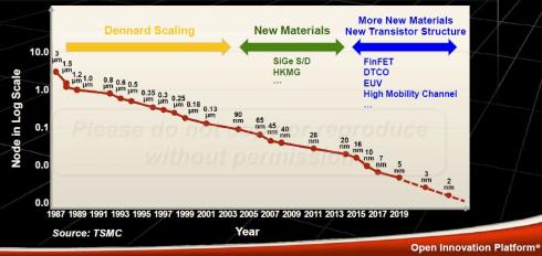
Dr. Y.-J. Mii, Senior Vice President of Research and Development / Technology Development , highlighted three eras of process technology development, as depicted in the figure below from his presentation.
In the first phase, Dennard scaling refers to the goal of scaling FEOL linear lithographic dimensions by a factor of “s” (s < 1) in successive process nodes, achieving an improvement of (1 / s**2) in circuit density, measured as gates / mm**2. The next phase focused on material improvements, and the current phase centers on design-technology co-optimization – more on that shortly.
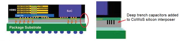
In a subsequent presentation at the symposium, Dr. Doug Yu, VP, Integrated Interconnect and Packaging R&D, described how advanced packaging technology has also been focused on scaling, albeit for a shorter duration. “For over 10 years, packages have also offered two-dimensional improvements to redistribution layer (RDL) and bump pitch lithography. With the multi-die, 3D vertical stacking package technology we’re describing today – specifically, TSMC’s SoIC offering – we are providing vast improvements in circuit density. S is equal to zero. Or, in other words, infinite scaling.” 😀 (Indeed, it is easy to foresee product technologies starting to use the metric “gates / mm**3” .)
Here is a brief recap of the TSMC advanced process technology status.
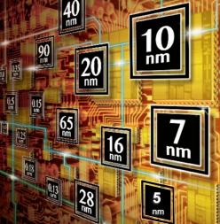
N7/N7+
TSMC announced the N7 and N7+ process nodes at the symposium two years ago. (link)
N7 is the “baseline” FinFET process, whereas N7+ offers improved circuit density with the introduction of EUV lithography for selected FEOL layers. The transition of design IP from N7 to N7+ necessitates re-implementation, to achieve a 1.2X logic gate density improvement. Key highlights include:
- N7 is in production, with over 100 new tapeouts (NTOs) expected in 2019
- Key IP introduction: 112Gbps PAM4 SerDes
- N7+ is benefitting from improvements in sustained EUV output power (~280W) and uptime (~85%). “Although we anticipate further improvements in power and uptime, these measures are sufficient to proceed to N7+ volume ramp.”, TSMC said.
- TSMC has focused on defect density (D0) reduction for N7. “The D0 improvement ramp has been faster than previous nodes, at a comparable interval after initial production volume ramp.”, according to TSMC.
- TSMC illustrated a dichotomy in N7 die sizes – mobile customers at <100 mm**2, and HPC customers at >300 mm**2.
- To my recollection, for the first time TSMC also indicated they are tracking D0 specifically for “large chips”, and reported a comparable reduction learning for large designs as for other N7 products.
- N7+ will enter volume ramp in 2H2019, and is demonstrating comparable D0 defect rates as N7.
“Making 5G a Reality”
TSMC invited Jim Thompson, CTO, Qualcomm, to provide his perspective on N7 – a very enlightening presentation:
- “N7 is the enabler for the 5G launch, as demonstrated in our latest Snapdragon 855 release.”
- “5G MIMO with 256 antenna elements supports 64 simultaneous digital streams – that’s 16 users each receiving 4 data streams to a single phone.”
- “Antenna design is indeed extremely crucial for 5G, to overcome path loss and signal blockage. There are new, innovative antenna implementations being pursued – in the end, it’s just math, although complex math for sure.”
- “There’s certainly lots of skepticism about the adoption rate of 5G. Yet 5G is moving much faster than 4G did – at a comparable point in the rollout schedule, there were only 5 operators and 3 OEM devices supporting 4G, mostly in the US and South Korea. Currently, there are over 20 operators and over 20 OEM devices focused on 5G deployment, including Europe, China, Japan, and Southeast Asia.”
- “And, don’t overlook the deployment of 5G in applications other than consumer phones, such as ‘wireless factory automation’. Communication to/from industrial robots requires high bandwidth, low latency, and extremely high availability. Consider the opportunities for manufacturing flexibility in a wire-free environment, enabled by 5G.”
N6
TSMC introduced a new node offering, denoted as N6. This node has some very unique characteristics:
- design rule compatible with N7 (e.g., 57mm M1 pitch, same as N7)
- IP models compatible with N7
- incorporates EUV lithography for limited FEOL layers – “1 more EUV layer than N7+, leveraging the learning from both N7+ and N5”
- tighter process control, faster cycle time than N7
- same EDA reference flows, fill algorithms, etc. as N7
- N7 designs could simply “re-tapeout” (RTO) to N6 for improved yield with EUV mask lithography
- or, N7 designs could submit a new tapeout (NTO) by re-implementing logic blocks using an N6 standard cell library (H240) that leverages a “common PODE” (CPODE) device between cells for an ~18% improvement in logic block density
- risk production in 1Q’20 (a 13 level metal interconnect stack was illustrated)
- although design rule compatible with N7, N6 also introduces a very unique feature – “M0 routing”
The figure below illustrates a “typical” FinFET device layout, with M0 solely used as a local interconnect, to connect the source or drain nodes of a multi-fin device and used within the cell to connect common nFET and pFET schematic nodes.
I need to ponder a bit more on the opportunity use M0 as a routing layer – TSMC indicated that EDA router support for this feature is still being qualified.
N6 strikes me as a continuation of TSMC’s introduction of a “half node” process roadmap, as depicted below.
A half-node process is both an engineering-driven and business-driven decision to provide a low-risk design migration path, to offer a cost-reduced option to an existing N7 design as a “mid-life kicker”.
The introduction of N6 also highlights an issue that will become increasingly problematic. The migration of a design integrating external IP is dependent upon the engineering and financial resources of the IP provider to develop, release (on a testsite shuttle), characterize, and qualify the IP on a new node on a suitable schedule. N6 offers an opportunity to introduce a kicker without that external IP release constraint.
N5
The process node N5 incorporates additional EUV lithography, to reduce the mask count for layers that would otherwise require extensive multipatterning.
- risk production started in March’19, high volume ramp in 2Q’20 at the recently completed Gigafab 18 in Tainan (phase 1 equipment installation completed in March’19)
- intended to support both mobile and high-performance computing “platform” customers; high-performance applications will want to utilize a new “extra low Vt”(ELVT) device
- 1.5V or 1.2V I/O device support
- an N5P (“plus”) offering is planned, with a +7% performance boost at constant power, or ~15% power reduction at constant perf over N5 (one year after N5)
- N5 will utilize a high-mobility (Ge) device channel
Advanced Materials Engineering
In addition to the N5 introduction of a high mobility channel, TSMC highlighted additional materials and device engineering updates:
- super high-density MIM offering (N5), with 2X ff/um**2 and 2X insertion density
- new low-K dielectric materials
- metal Reactive Ion Etching (RIE), replacing Cu damascene for metal pitch < 30um
- a graphene “cap” to reduce Cu interconnect resistivity
An improved local MIM capacitance will help to address the increased current from the higher gate density. TSMC indicated an expected single-digit % performance increase could be realized for high-performance (high switching activity) designs.
Nodes 16FFC and 12FFC both received device engineering improvements:
- 16FFC+ : +10% perf @ constant power, +20% power @ constant perf over 16FFC
- 12FFC+ : +7% perf @ constant power, +15% power @ constant perf over 12FFC
NTO’s for these nodes will be accepted in 3Q’19.
TSMC also briefly highlighted ongoing R&D activities in materials research for future nodes – e.g., Ge nanowire/nanoslab device channels, 2D semiconductor materials (ZrSe2, MoSe2) – see the figure below (Source: TSMC).
Manufacturing Excellence
Dr. J.K. Wang, SVP, Fab Operations, provided a detailed discussion of the ongoing efforts to reduce DPPM and sustain “manufacturing excellence”. Of specific note were the steps taken to address the demanding reliability requirements of automotive customers. Highlights of Dr. Wang’s presentation included:
“Since the introduction of the N16 node, we have accelerated the manufacturing capacity ramp for each node in the first 6 months at an ever-increasing rate. The N7 capacity in 2019 will exceed 1M 12” wafers per year. The N10/N7 capacity ramp has tripled since 2017, as phases 5 through 7 of Gigafab 15 have come online.”
“We have implemented aggressive statistical process control (measured on control wafer sites) for early detection, stop, and fix of process variations – e.g., upward/downward shifts in baseline measures, a variance shift, mismatch among tools. We have established 2D wafer profile measurement criteria, and in-line monitoring and comparison to an “acceptance” profile across each wafer.”
“The DDM reduction rate on N7 has been the fastest of any node.”
“For automotive customers, we have implemented unique measures to achieve the demanding DPPM requirements. We will ink out good die in a bad zone. And, there are SPC criteria for a maverick lot, which will be scrapped.”
“We will support product-specific upper spec limit and lower spec limit criteria. We will either scrap an out-of-spec limit wafer, or hold the entire lot for the customer’s risk assessment.” (See the figures below. Source: TSMC)
Automotive Platform
TSMC has developed an approach toward process development and design enablement features focused on four platforms – mobile, HPC, IoT, and automotive. Dr. Cheng-Ming Lin, Director, Automotive Business Unit, provided an update on the platform, and the unique characteristics of automotive customers.
Growth in semi content
Dr. Lin indicated, “Automotive systems will require both advanced logic technologies for ADAS, such as N16FFC, and advanced RF technologies for V2X communications. Although the CAGR for cars from now to 2022 is expected to be only ~1.8%, the CAGR for the semiconductor content will be 6.9%.”
He continued, “The L1/L2 feature adoption will reach ~30%, with additional MCU’s applied to safety, connectivity, and EV/hybrid EV features. There will be ~30-40 MCU’s per vehicle. “ (In his charts, the forecast for L3/L4/L5 adoption is ~0.3% in 2020, and 2.5% in 2025.)
“The adoption rate for the digital dashboard cockpit visualization system will also increase, driving further semiconductor growth – 0.2% in 2018 to 11% in 2025.”
L2+
The levels of support for automated driver assistance and ultimately autonomous driving have been defined by SAE International as “Level 1 through Level 5”. Perhaps in recognition of the difficulties in achieving L3 through L5, a new “L2+” level has been proposed (albeit outside of SAE), with additional camera and decision support features.
“An L2+ car would typically integrate 6 cameras, 4 short-range radar systems, and 1 long-range radar unit, requiring in excess of 50GFLOPS graphics processing and >10K DMIPS navigational processing throughput.”
N16FFC, and then N7
The 16FFC platform has been qualified for automotive environment applications – e.g., SPICE and aging models, foundation IP characterization, non-volatile memory, interface IP. The N7 platform will be (AEC-Q100 and ASIL-B) qualified in 2020. “Automotive customers tend to lag consumer adoption by ~2-3 years, to leverage DPPM learning – although that interval is diminishing. We anticipate aggressive N7 automotive adoption in 2021.”,Dr. Lin indicated.
“The TSMC RF CMOS offerings will be used for SRR, LRR, and Lidar. The 16FFC-RF-Enhanced process will be qualified for automotive platforms in 2Q’20.”
IoT Platform
The TSMC IoT platform is laser-focused on low-cost, low (active) power dissipation, and low leakage (standby) power dissipation. Dr. Simon Wang, Director, IoT Business Development, provided the following update:
Process Roadmap
- 55ULP, 40ULP (w/RRAM): 0.75V/0.7V
- 22ULP, 22ULL: 0.6V
- 12FFC+_ULL: 0.5V (target)
- introduction of new devices for the 22ULL node: EHVT device, ultra-low leakage SRAM
The 22ULL SRAM is a “dual VDD rail” design, with separate logic (0.6V, SVT + HVT) and bitcell VDD_min (0.8V) values for optimum standby power.
The 22ULL node also get an MRAM option for non-volatile memory.
Note that a new methodology will be applied for static timing analysis for low VDD design. The stage-based OCV (derating multiplier) cell delay calculation will transition to sign-off using the Liberty Variation Format (LVF).
The next generation IoT node will be 12FFC+_ULL, with risk production in 2Q’20. (with low VDD standard cells at SVT, 0.5V VDD).
RF
TSMC emphasized the process development focus for RF technologies, as part of the growth in both 5G and automotive applications. Dr. Jay Sun, Director, RF and Analog Business Development provided the following highlights:
- For RF system transceivers, 22ULP/ULL-RF is the mainstream node. For higher-end applications, 16FFC-RF is appropriate, followed by N7-RF in 2H’20.
- Significant device R&D is being made to enhance the device ft and fmax for these nodes – look for 16FFC-RF-Enhanced in 2020 (fmax > 380GHz) and N7-RF-Enhanced in 2021.
- New top-level BEOL stack options are available with ‘elevated’ ultra thick metal for inductors with improved Q.
- For sub-6GHz RF front-end design, TSMC is introducing N40SOI in 2019 – the transition from 0.18um SOI to 0.13um SOI to N40SOI will offer devices with vastly improved ft and fmax.
Summary
There was a conjecture/joke going around a couple of years ago, suggesting that “only 7 customers will be able to afford to pursue 7nm designs, and only 5 customers at 5nm”.
Clearly, the momentum behind N7/N6 and N5 across mobile communication, HPC, and automotive (L1-L5) applications dispels that idea. TSMC is investing significantly in enabling these nodes through DTCO, leveraging significant progress in EUV lithography and the introduction of new materials.
Part 2 of this article will review the advanced packaging technologies presented at the TSMC Technology Symposium.
-chipguy
Also read: TSMC Technology Symposium Review Part II