There is a report in the Seoul Economic Daily that Samsung has completed development of their 7nm process using EUV and that production will begin in June. What is claimed in the report is:
- The process is installed in the Hwaseong S3 Fab
- Samsung has more than 10 EUV systems installed
- Production starts in June with Qualcomm, Xilinx, Apple and HiSilicon as customers (Authors correction: the original article was in Korean and the source I used got the translation wrong, apparently only Qualcomm was listed in the original article)
Initially when I read this I was skeptical, but the more I have thought about it and investigated the various elements of this claim, the more I have come to believe this report is largely true. The following is my rational:
According to my tracking of 300mm wafer fabs as published in the IC Knowledge 300mm Watch Database, the Hwaseong fab has 4 phases. Phase 1 is for DRAM, phase 2 is for 3D NAND, phase 3 and phase 4 are know as S3 phase 1 and 2 and are for logic. Phase 1 is 10nm and phase 2 for 7nm. The S designation is used by Samsung for their foundry logic fabs. This fab “cluster” is also known to be Samsung’s EUV hub so 7nm production with EUV in “S3” makes sense and is consistent with this site and our expectations for how it will be used.
I gave a talk on EUV at ISS this year that I wrote up here. While researching EUV status for that talk I tried to determine where every EUV system installed to-date is located. It was my conclusion that Samsung had approximately 10 EUV systems installed consistent with the more than 10 EUV system installed assertion in the article.
The biggest surprise in this article is the idea that development of 7nm with EUV is done. At the SPIE Advanced Lithography Conference this year it seemed like everyone just woke up to the stochastic issues with EUV (I wrote that up here).
Simply put, dose is given by:
EUV photons have roughly 10x the energy of deep UV photons and for the same dose there is roughly 10x fewer EUV photons. This contributes to a variety of stochastic effects such as shot noise and photoresist issues. There is however a simple fix to this – run a higher dose. The problem with running a higher dose is the impact on throughput.
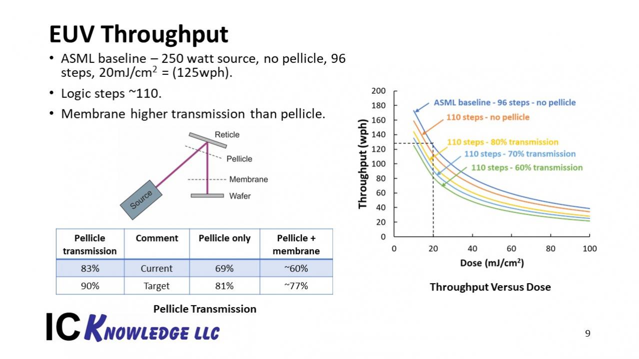
The following slide from my ISS talk illustrates the effect of dose on throughput.

Figure 1. EUV Throughput
To-date the throughput numbers that ASML has published are based on a 20mJ/cm[SUP]2[/SUP] dose with 96 steps and no pellicle. Logic devices generally require around 110 steps and Samsung is expected to be using EUV for metal layers, so they will need a pellicle. I have been hearing rumors that Samsung is using a 50mJ/cm[SUP]2[/SUP] dose. The overall impact of the higher dose, pellicle and more steps is that throughput will only be around 60 wafers per hour (wph) (please note that since this slide was created ASML has achieved 140 wph for 96 steps, 20mJ/cm2 and no pellicle).
Assuming Samsung is in fact running at 50mJ/cm[SUP]2[/SUP] that may be sufficient to get around most of the worst stochastic issues and produce a usable process.
The question then becomes would they be willing to accept such low throughput and therefore increased costs. Once again there is a relevant rumor and that is that “foundries” are accepting that they may have to absorb higher initial costs for EUV wafers. Samsung is also a company that is rumored to use brute force to get a process started. At 10nm it was said that in the beginning when yields were low that they simply ran a lot of wafers to get shippable parts. Perhaps in order to get EUV started they will accept low throughput and high costs to be first to production and to start the high-volume learning process.
The combination of what is known about EUV and the rumors about Samsung make me believe that we will in fact see Samsung begin to ship 7nm wafers using EUV starting in June. Likely this will be by running the EUV systems in a way that delivers low throughput and high costs and there may be yield issues as well, but this will make Samsung the first to enter production with EUV.
I will say the customer list surprises me, I thought Apple was at TSMC for 100% of their 7nm business and I thought Qualcomm and Xilinx were also TSMC 7nm customers. But the rest of this report is credible in my opinion.
Share this post via:


Captain America: Can Elon Musk Save America’s Chip Manufacturing Industry?