It is truly amazing to consider the advances in microelectronic process development, using 193i photolithography. The figure below is a stark reminder of the difference between the illuminating wavelength and the final imaged geometries. This technology evolution has been enabled by continued investment in mask data generation (including multipatterning decomposition) and exposure optimizations, generally known as computational lithography.

This technology evolution has also resulted in increasing complexity in drawn layout design rules, due to the optical interaction between neighboring geometries — data both on the same layer and different layers — as well as the greater impact of manufacturing process mask overlay and fabrication variations. In short, the traditional layout design rule manual, and the corresponding DRC code implementations, have been augmented by a complementary set of layout topology checks.
The IC industry has used several terms to refer to these additional verification methods — i.e., Design for Manufacturability(DFM), Design for Yield (DFY, often merged into one, as DFM/DFY), and Lithography Process Checks (LPC, aka Litho Friendly Design, or LFD). For the purposes of this discussion, we’ll rely more on the terms rule-based and model simulation-based checks.
I recently had the opportunity to chat with Michael White, Director of Product Marketing, Calibre Physical Verification at Mentor Graphics, and K.K. Lin, Director of Foundry Marketing Ecosystem, at Samsung Semiconductor, and learned of several interesting new developments and methodologies in the area of rule-based checking. Specifically, both Michael and K.K. highlighted the growing body of applications for layout pattern matching algorithms, as embodied in Mentor’s Calibre Pattern Matching product.
Patterns Applied for DRC
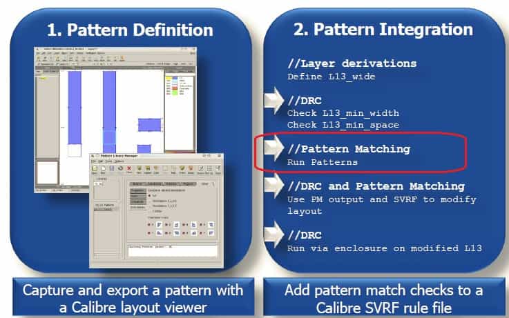
Michael provided a unique perspective, saying, “Calibre is really an application development platform, built upon industry-leading geometrical processing algorithms and database management technology. As the demand grew to represent complex layout rule checks graphically, rather than as a sequence of text-based (SVRF) operations, it was straightforward to integrate Calibre pattern matching capabilities into the Calibre design rule checking flow.” The figure below illustrates how a checking deck is easily modified.
The error markers associated with the library of patterns are displayed in the familiar Calibre Results Viewing Environment (RVE).
“In addition to representing complex checks at advanced nodes, we’re seeing patterns applied to DRC layout validation at older process nodes.”, Michael added. “There are lots of new design starts at established nodes for new application markets. The twist is that these designs are often incorporating new sensor-based functionality, such as MEMS structures combined with new mixed-signal circuits. These structures often utilize curvilinear layout geometries. Design rule checks added to support these new elements in existing processes are often simply included using the Calibre pattern matching capabilities.”
Patterns to Accelerate Model-Based Checking
At advanced nodes, the illumination source and mask optimizations (SMO) applied during mask data generation have become so complex that it became necessary for designers to confirm prior to tapeout that this step would be successful post-tapeout. A model simulation-based methodology was defined, commonly known as lithography process checking, and added to the tapeout release flow.
These computationally-intensive algorithms, exercised by a tool such as Calibre LFD, look for “hot spots” that could be problematic for SMO.
To address the demanding amount of compute resources required for LFD, pattern matching techniques are used to filter and find only those layout geometries that warrant further (model-based) analysis. “Using Calibre pattern matching, 90% of the layout can typically be excluded from LFD — only 10% of the design is simulated.”, Michael highlighted.
What is a Pattern?
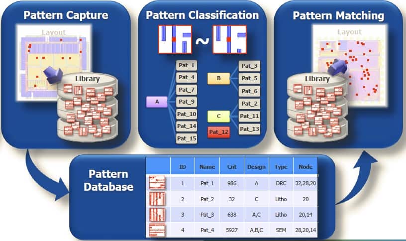
Layout patterns are a local geometric relationship among shapes/edges, spanning one or many mask layers. They can be generated in several ways:
- hand-drawn
- a “clip” from an existing layout cell (either manually or automatically-generated)
- extensions to an existing pattern, adding variability to allowed movement of (single or paired) edges
Specific Calibre RVE error markers are added to the pattern, as well.

As illustrated above, the Calibre platform also includes support to reduce the raw volume of (fixed-match) patterns, with tools to apply a superset classification when constructing the pattern library.
Patterns and Samsung’s Closed-Loop DFM Yield Enhancement Flow
Perhaps the most prevalent application of pattern matching is to identify potential yield detracting layouts — i.e., designs that pass DRC and LPC verification, yet are high on the pareto chart of manufacturing yield-limiting topologies. This pre-tapeout analysis step is more subjective — rather than a pass/fail result, design matching patterns can be assigned a score to indicate the criticality of the topologies. Tapeout signoff involves a review of the scoring data, to determine if process margins are sufficient and/or if design improvements are needed.
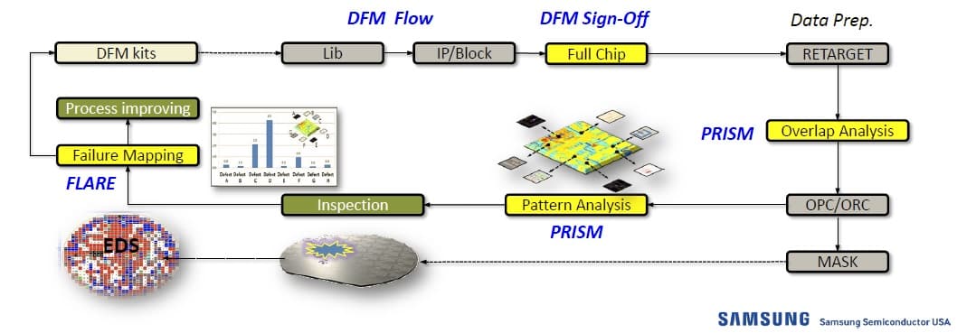
Using the Mentor Calibre and Tessent design-for-testability tool platforms, Samsung has internally developed a methodology to apply manufacturing production learning to the development of DFM library kits for customer use pre-tapeout. This comprehensive closed-loop DFM flow is illustrated in the figure below.

K.K. Lin described two key Samsung tools that anchor this methodology. Subsequent to the customer’s DFM tapeout review signoff, Samsung PRISM (Pattern Recognition and Identity Scoring Method) is applied. The first usage analyzes the initial mask data for design critical topologies, with the output fed to the optical correction algorithms. Key examples of the pattern matching analysis performed at this step examine the overlap of contacts/vias.
The second invocation of PRISM provides single-layer pattern analysis results to input to the in-line mask inspection tooling. The tool can use this information to enhance mask inspection parameters on specific yield-critical features — tighter specifications for production mask plate inspection in critical areas will optimize throughput while maintaining high yield. (Note that the patterns used in this context could be very complex and intricate, as this is applied to optically-corrected mask data.)
Samsung’s second tool in the closed-loop DFM optimization flow is FLARE, for Failure anaLysis And yield Rank Estimation. Utilizing the manufacturing defect isolation and logical-to-physical mapping technology within Mentor’s Tessent platform, post-silicon physical failure analysis applies the deep learning features of FLARE to identify and prioritize yield-detracting structures. The FLARE results, from both process test vehicles and existing products, are used to identify areas for ongoing process improvement and/or the addition of new patterns to the DFM kit provided to customers. K.K. indicated, “With the application of this closed-loop DFM flow, we have seen product yield improvements of 10% or more.” (Wow!)
The complexity of modern lithographic mask data generation requires focus on (rule-based and model-based) methods for verifying the manufacturability and yield or an increasing diversity of chip designs. Pattern matching technology, such as with Mentor Calibre Pattern Matching, is seeing increasing application, whether as: an extension to traditional text-based DRC check operations; a filter for computationally-intensive (pre-tapeout) lithography process checking; or, as part of yield learning and optimization, as exemplified by Samsung’s DFM methodology. Pattern matching is thus both an enabler for process node development, and a key facet of production cost reduction.
A link to a wealth of information on Mentor Calibre Pattern Matching is available here.
If you will be attending DAC 2016 in Austin, I would encourage you to sign up for a lunch seminar and a DAC exhibit presentation on this technology, and how Samsung has achieved significant process improvement and yield optimization:
- Mentor-Samsung lunch seminar: “Accelerate Yield Ramps with Samsung Foundry Closed-Loop DFM and Mentor tools”, Monday, June 6, 12:00 –1:30 PM. Please register using this link.
- Mentor Calibre Pattern Matching presentation: “Pattern Matching Applications Are Exploding—And Solving Tough Problems”, Tuesday, 3PM, Mentor Graphics DAC booth #949
-chipguy
Share this post via:


Comments
0 Replies to “Layout Pattern Matching for DRC, DFM, and Yield Improvement”
You must register or log in to view/post comments.