Last week I wrote about the Photonics Summit and hands-on training hosted by Cadence Design, PhoeniX Software and Lumerical Solutions and in that article I mentioned that Ted Letavic of Global Foundries laid out a powerful argument for why integrated photonics is a technology that is going main stream. This article dives into … Read More

Always-On IoT – FDSOI’s Always Better? What About Wafers? (Questions from Shanghai)
Mahesh Tirupattur, EVP at low-power SERDES pioneer Analog Bits lead off the panel discussion at the recent FD-SOI Forum in Shanghai with the assertion that for anything “always on” in IoT, FD-SOI’s always better. They had a great experience porting their SERDES IP to 28nm FD-SOI (which they detailed last spring – see the ppt here… Read More
New Cortex-M7 Chip to Help Power Sophisticated IoT Solutions
IoT architects face a dilemma in partitioning the compute power of their systems between the cloud and the edge. The cloud offers large storage and heavy duty compute power, making it an attractive place to perform the computation needed for IoT tasks. However, moving large amounts of data from the edge to the cloud servers, can … Read More
2016 semiconductor capex highest in 5 years
Global semiconductor capital expenditures (capex) are expected to return to the level of 2011 either this year or next. 2011 was the record year for capex as the industry returned to growth following the 2009-2010 recession. IC Insights’ August 2016 forecast called for 3.5% growth in capital spending to reach $67.1 billion, the… Read More
Foundry is Majority of KLAC Business!
As we had projected, with KLA having the highest exposure to foundry/logic of any tool company, they are seeing the most near term strength as foundries (read that as TSMC) spend big for 10NM and 7NM. In addition the first tools you buy are yield management/metrology tools which KLA is the king of.
KLA put up numbers well above estimates….Generating… Read More
Foundry CAPEX Jumped from 17% to 37% of LAM Business
Lam- in line qtr but guides above street over near term. As with ASML, foundry is driver with subdued memory, The Math implies biz peaking-Looking for DRAM in 2017.
Lam reported another great, record quarter, more or less in line with expectations with revenues coming in at $1.632B and shipments of $1.708B, generating EPS of $1.81.… Read More
What is the impact of missing the 7NM node with EUV?
ASML reported a quarter that was slightly below expectations coming in at Euro 1.815B in revenues and Euro 0.93 EPS. Orders were a bit soft at Euro 1.4B but well within the normal quarterly variation of a lumpy business. Euro 28M was lost in a currency adjustment associated with the Hermes acquisition.
The guidance for Q4 was between… Read More
What’s the Intel Capex Outlook?
Intel has terrific QTR & slightly light guide Intel is recovering & transforming at the same time. Whats the Capex outlook? Impact on ASML KLAC LRCX?
Intel reported revenues of $15.78B and earnings of $0.80 for the quarter beating expectations and previous upward guidance. CCG (PCs) were up 21% Q/Q and 5% Y/Y. Data center… Read More
Webinar Offers View into TSMC IP Design Methodology
Standard cell and memory IP are key enablers for new process node availability. These two items must be in place early and be completely ready for a process node to scale to volume. Development of both leaves no room for error and they require the highest performance possible. Foundries are extremely focused on this and spend a lot… Read More
The Fabless Empire Strikes Back, Global Foundries and Cadence make moves into Integrated Photonics!
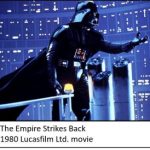
In August I wrote an article proclaiming Score 1 for IDMs vs Fabless and discussedIntel’sannouncement of volume production of their 100G PSM4 and 100G CWDM4 transceiver products.
This week the Fabless Empire strikes back.Daniel Nenni and I attended a two-day Photonic Summit and workshop hosted by Cadence Design, PhoeniX Software… Read More
Enhancing Multi-Domain System Simulation with FMI Co-Simulation