You are currently viewing SemiWiki as a guest which gives you limited access to the site. To view blog comments and experience other SemiWiki features you must be a registered member. Registration is fast, simple, and absolutely free so please,
join our community today!
WP_Term Object
(
    [term_id] => 158
    [name] => Semiconductor
    [slug] => semiconductor-manufacturers
    [term_group] => 0
    [term_taxonomy_id] => 158
    [taxonomy] => category
    [description] =>
    [parent] => 0
    [count] => 1407
    [filter] => raw
    [cat_ID] => 158
    [category_count] => 1407
    [category_description] =>
    [cat_name] => Semiconductor
    [category_nicename] => semiconductor-manufacturers
    [category_parent] => 0
    [is_post] =>
)
On their first quarter earnings call Intel announced that volume production of 10nm has been moved from the second half of 2018 to 2019 due to yield issues. Specifically, they are shipping 10nm in low volume now, but yield improvement has been slower than anticipated. They report that they understand the yield issues but that improvements… Read More
Intel (INTC) blew away expectations based on strong performance in the data center. Revenues of $16.1B versus street of $15.05B and EPS of $0.93 versus street of $0.72. While revenue was up 9% over prior year, earnings were 50% higher. Guidance is for Q2 revenue of $16.3B and EPS of $0.85 versus street of $15.55B and EPS of $0.81. IOT,… Read More
Samsung throws further gas on the fire of weak handset and CAPEX not set but will be down versus 2017. Samsung reported revenues of KRW 60.56 Trillion and KRW 15.64 Trillion operating profit ($56B and $15B). Chips accounted for whopping KRW 11.55 Trillion in operating profit on revenues of KRW 20.78 Trillion ( $11B and $19B)….a… Read More
There is a report in the Seoul Economic Daily that Samsung has completed development of their 7nm process using EUV and that production will begin in June. What is claimed in the report is:
- The process is installed in the Hwaseong S3 Fab
- Samsung has more than 10 EUV systems installed
- Production starts in June with Qualcomm, Xilinx,
…
Read More
I was invited to give a talk at the Business of Cleans Conference held by Linx Consulting in Boston on April 9th. I am not a cleans expert but rather was invited more to give an overview talk on process technology trends and the impact on cleans. In this write up I will discuss my presentation. I discussed each of the three main leading-edge… Read More
It has been reported over the holiday weekend that Intel is in talks with Micron over a proposed merger that would value Micron at $70 per share in a deal of a combination of stock and cash for Micron shareholders. It is said that the boards of both companies have already approved the deal.
Intel’s CEO Brian Krzanich said, “We… Read More
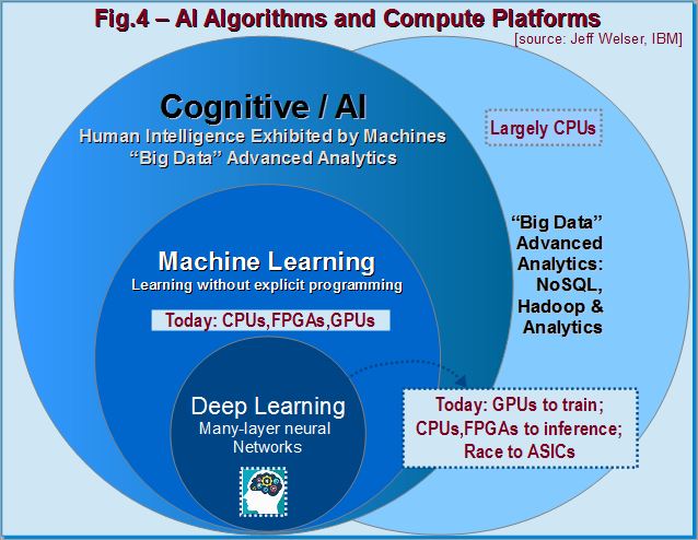
Adding color to the talks, Dr. Jeff Welser, VP and IBM Almaden Research Lab Director showed how AI and recent computing resources could be harnessed to contain data explosion. Unstructured data growth by 2020 would be in the order of 50 Zetta-bytes (with 21 zeros). One example, the Summit supercomputer developed by IBM for use at… Read More
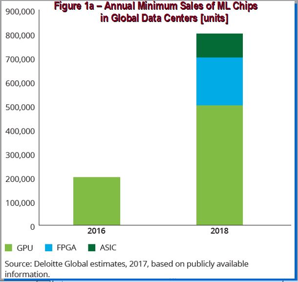
Just like good ideas percolate longer, we have seen AI adoption pace picking-up speed, propelled by faster GPUs. Some recent data points provide good indication that FPGA making a comeback to bridge chip-design needs to keep-up with AI’s ML applications.
According to the Deloitte research firm there is a projected increase of… Read More
The most viewed blogs I write for SemiWiki are consistently blogs comparing the four leading edge logic producers, GLOBALFOUNDRIES (GF), Intel, Samsung (SS) and TSMC. Since the last time I compared the leading edge new data has become available and several new processes have been introduced. In this blog I will update the current… Read More
This year the Advanced Lithography Conference felt very different to me than the last couple of years. I think it was Chris Mack who proclaimed it the year of Stochastics. EUV has dominated the conference for the last several years but in the past the conversation has been mostly centered on the systems, system power and uptime.
I … Read More


Enhancing Multi-Domain System Simulation with FMI Co-Simulation