You are currently viewing SemiWiki as a guest which gives you limited access to the site. To view blog comments and experience other SemiWiki features you must be a registered member. Registration is fast, simple, and absolutely free so please,
join our community today!
WP_Term Object
(
    [term_id] => 158
    [name] => Semiconductor
    [slug] => semiconductor-manufacturers
    [term_group] => 0
    [term_taxonomy_id] => 158
    [taxonomy] => category
    [description] =>
    [parent] => 0
    [count] => 1406
    [filter] => raw
    [cat_ID] => 158
    [category_count] => 1406
    [category_description] =>
    [cat_name] => Semiconductor
    [category_nicename] => semiconductor-manufacturers
    [category_parent] => 0
    [is_post] =>
)
At the 2024 TSMC OIP Ecosystem Forum, one of the technical talks by TSMC focused on maximizing 3DIC design productivity and rightfully so. With rapid advancements in semiconductor technology, 3DICs have become the next frontier in improving chip performance, energy efficiency, and density. TSMC’s focus on streamlining the… Read More
Synopsys made significant announcements during the recent TSMC OIP Ecosystem Forum, showcasing a range of cutting-edge solutions designed to address the growing complexities in semiconductor design. With a strong emphasis on enabling next-generation chip architectures, Synopsys introduced both new technologies and … Read More
Even though this is the 16th OIP event please remember that TSMC has been working closely with EDA and IP companies for 20+ years with reference flows and other design enablement and silicon verification activities. The father of OIP officially is Dr. Morris Chang who named it the Grand Alliance. However, Dr. Cliff Hou is the one … Read More
The 2024 live conferences have been well attended thus far and there are many more to come. The next big event in Silicon Valley is the TSMC Global OIP Ecosystem Forum on September 25th at the Santa Clara Convention Center. I expect a big crowd filled with both customers and partners.
This is the 16th year of OIP and it has been an honor… Read More
The Universal Chiplet Interconnect Express™ (UCIe™) 1.0 specification was announced in early 2022 and a UCIe 1.1 update was released on August 8, 2023. This open standard facilitates the heterogeneous integration of die-to-die link interconnects within the same package. This is a fancy way of saying the standard opens the door… Read More
Can a 4-member alliance reshape the semiconductor industry?
Semiconductors are ubiquitous in electronics and computing devices, making them essential to developments in AI, advanced military, and the world economy. As such, it is unquestionable that nations attain considerable … Read More
If you work in the Semiconductor or related industry, you know that industry cycles can profoundly impact your business. It is crucial for strategic development to invest at the appropriate time and to rope the sails when necessary.
As a semiconductor investor, you’re accustomed to the ebb and flow of industry cycles. It’s… Read More
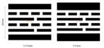
At IEDM 2019, TSMC revealed two versions of 5nm standard cell layouts: a 5.5-track DUV-patterned version and a 6-track EUV-patterned version [1]. Although the metal pitches were not explicitly stated, later analyses of a 5nm product, namely, Apple’s A15 Bionic chip, revealed a cell height of 210 nm [2]. For the 6-track … Read More
At #61DAC our very own Daniel Nenni from SemiWiki moderated an informative panel discussion on the topic of 3D IC Design Ecosystem. Panelists included: Deepak Kulkarni – AMD, Lalitha Immaneni – Intel Foundry, Trupti Deshpande – Qualcomm, Rob Aitken – CHIPS, Puneet Gupta – UCLA, Dragomir Milojevic – imec. Each panelist had a brief… Read More
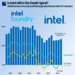
Does this justify the widespread Intel bashing?
The latest Intel earnings release was another sharp and deeper turn into the company’s death spiral. On the surface, it is just a whole load of bad news, and the web has been vibrating with Intel bashing since the release.
So what are the facts?
From a revenue perspective, Intel was inside… Read More


Podcast EP357: How Gonka is Changing the Way AI is Accessed with David Liberman