
I purchased two Toyotas last year and both have since been recalled. Why has Toyota spent $1B+ on recalls in recent years? Same reason why it will cost Intel $700M (which does not include reputation damage) to recall Sandy Bridge chip sets, because someone did not do their job! The WHAT has been discussed, lets talk about HOW it happened.

Intel Identifies Chipset Design Error, Implementing Solution
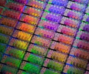
SANTA CLARA, Calif., Jan. 31, 2011 – As part of ongoing quality assurance, Intel Corporation has discovered a design issue in a recently released support chip, the Intel® 6 Series, code-named Cougar Point, and has implemented a silicon fix. In some cases, the Serial-ATA (SATA) ports within the chipsets may degrade over time, potentially impacting the performance or functionality of SATA-linked devices such as hard disk drives and DVD-drives. The chipset is utilized in PCs with Intel’s latest Second Generation Intel Core processors, code-namedSandyBridge. Intel has stopped shipment of the affected support chip from its factories. Intel has corrected the design issue, and has begun manufacturing a new version of the support chip which will resolve the issue. TheSandyBridgemicroprocessor is unaffected and no other products are affected by this issue.
Coincidently Mentor Graphics recently published an article:

New ERC Tools Catch Design Errors that Lead to Circuit Degradation Failures
Published on 02-11-2011 12:18 PM: A growing number of reports highlight a class of design errors that is difficult to check using more traditional methods, and can potentially affect a wide range of IC designs, especially where high reliability is a must.Today’s IC designs are complex. They contain vast arrays of features and functionality in addition to multiple power domains required to reduce power consumption and improve design efficiency. With so much going on, design verification plays an important role in assuring that your design does what you intended. Often, verification will include simulations (for functional compliance), and extensive physical verification (PV) checks to ensure that the IC has been implemented correctly, including DRC, LVS, DFM and others. A growing number of reports highlight a class of design errors that is difficult to check using more traditional methods, and can potentially affect a wide range of IC designs, especially where high reliability is a must.
Note the comment by SemiWiki Blogger Daniel Payne, who used to work at both Intel and Mentor Graphics:

A transistor-level checking tool like PERC can certainly catch reliability failure issues like a PMOS transistor with bulk node tied to the wrong supply (let’s say 2.5V instead of 1.1V).
Since Intel announced that a single transistor reliability issue is to blame for their recent re-spin, we can only guess at the actual reliability issue that they found and fixed with a single metal layer.
I’m sure that at Intel for all new chips they will be running their reliability tool checks before tape out instead of during fabrication.
Back in the 1980’s Intel did have an internal tool called CLCD (Coarse Level Circuit Debugger) that could crawl a transistor netlist and look for any configuration. You would write rules for each reliability or circuit issue that you knew of, then run your netlist in CLCD to detect them.

Now for the HOW: Based on my personal experience, Intel has a classic case of the NIH (not invented here) Syndrome when it comes to EDA tools and methodologies. Even when Intel purchases commercial EDA tools they are often not used in the prescribed methodology. Intel also does not collaborate well with vendors and is very secretive in the usage of purchased tools. Bottom line: Someone at Intel did not do their job. Just my opinion of course but this $700M fiasco could have and should have been avoided.
Share this post via:


Comments
0 Replies to “Intel Sandy Bridge Fiasco and EDA”
You must register or log in to view/post comments.