In an era dominated by artificial intelligence (AI), machine learning (ML), and high-performance computing (HPC), the demand for semiconductors that deliver high data throughput, low latency, and energy efficiency has never been greater. Traditional chip designs often struggle to keep pace with these requirements, leading to bottlenecks in performance and scalability. Intel Foundry’s Embedded Multi-Die Interconnect Bridge (EMIB) is a groundbreaking 2.5D interconnect technology that redefines chip packaging. Introduced in high-volume manufacturing since 2017, EMIB enables the seamless integration of multiple dies into a single package, enhancing performance, power efficiency, and design flexibility. This innovation addresses the limitations of monolithic chips by allowing heterogeneous integration, combining dies from different process nodes, without necessitating complete system redesigns.
At its core, EMIB employs small silicon bridges embedded within an organic substrate to facilitate high-bandwidth communication between adjacent dies. Unlike conventional approaches that rely on large silicon interposers, which embed multiple routing layers and require all signals and power vias to pass through them, EMIB uses a compact bridge with targeted microbump pitches. As illustrated in the technology brief, this design maintains a tight pitch only at the bridge interface, while the rest of the die-core region can retain a looser pitch, optimizing cost and efficiency. The manufacturing process aligns with standard semiconductor package-assembly flows, with the key difference being the substrate fabrication: bridges are placed in cavities, secured with adhesives, and layered with dielectrics and metals. This method not only reduces the footprint but also preserves input/output (I/O) signal integrity and power characteristics, avoiding the thermal and electrical challenges posed by full interposers.
EMIB’s advantages extend beyond its architecture. It supports high-data-rate signaling with simple driver/receiver circuitry, enabling customizable layouts for large, heterogeneous die complexes. Each die-to-die link can be optimized individually, tailoring bridges to specific interconnect needs, such as logic-logic or logic-high-bandwidth memory (HBM) communications. In response to evolving demands, Intel has expanded the EMIB portfolio. EMIB-M incorporates Metal Insulator Metal (MIM) capacitors into the bridges to improve power delivery, mitigating noise in high-power applications. Meanwhile, EMIB-T introduces through-silicon vias (TSVs) for vertical power delivery, enhancing compatibility with HBM and facilitating conversions from other packaging technologies. These variants achieve assembly yields comparable to standard flip-chip ball grid arrays (FCBGA), making them viable for high-volume production using both Intel and external silicon.
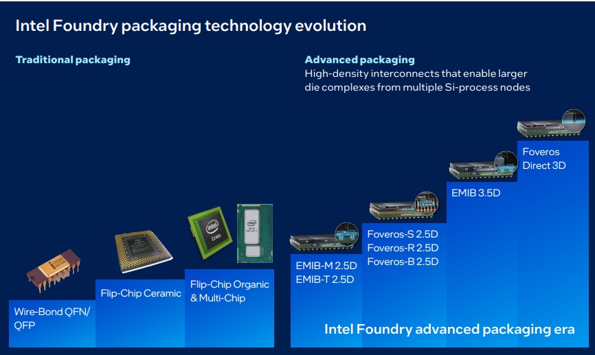
The true potential of EMIB unfolds when combined with Intel’s Foveros die-stacking technology, creating EMIB 3.5D—a hybrid architecture that merges 2.5D lateral bridging with 3D vertical stacking. This “system of chips” approach overcomes challenges like thermal warping, reticle size limits, and interconnect constraints, expanding the silicon surface area for complex systems. As depicted in the evolution from traditional wire-bond packages to advanced solutions, EMIB 3.5D balances package size, compute performance, power usage, and cost, making it ideal for AI accelerators and HPC workloads. By enabling disaggregated chiplet-based designs, it accelerates time-to-market and supports standards like UCIe for die-to-die interfaces.
Intel Foundry’s role as a pioneer in this space cannot be overstated. Through its Advanced System Assembly & Test (ASAT) division, it offers end-to-end solutions, including testing services and ecosystem partnerships for systems technology co-optimization (STCO). This shift from “system on chip” to “systems of chips” positions Intel at the forefront of the semiconductor industry’s transformation, fostering innovation in diverse sectors like servers, networks, and edge computing.
Bottom line: EMIB represents a paradigm shift in chip packaging, empowering designers to build more powerful, efficient, and scalable systems. As applications like AI continue to push boundaries, technologies like EMIB will be instrumental in driving progress, ensuring that computational demands are met with ingenuity and precision. With ongoing advancements, Intel Foundry is not just adapting to the future—it’s shaping it.


Comments
There are no comments yet.
You must register or log in to view/post comments.