I just read this very interesting article posted by Kurt Shuler from Arteris, describing the “History of SoC Interconnect Fabric” and explaining why the SC industry needs an advanced approach, named the “fourth phase of the Interconnect Fabric history” in the article. Kurt’s point of view is that in the past the SoC interconnect did not receive the type of research and development focus that CPUs or GPUs received. If you do not really understand what type of functionality is behind the “SoC Interconnect” or “Network-on-Chip” terms, you will certainly benefit from reading this article.

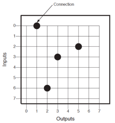
An 8-port unidirectional crossbar switch with four simultaneous connections (Source:Lattice Semiconductor)
The author starts from the beginning, when on-chip interconnect buses like AMBA or OCP were the only solution to interconnect the various functions within a SoC, and explains how the SC industry has evolved from buses to Crossbars, in the 1995-2005, to finally moved on to implement Network-on Chip (NoC) starting around the 2010’s. If you are already familiar with the NoC concept, you will benefit from the questions raised in this article: Do you need to explain to your management why investing in NoC IP is a smart thing? You may want to explain that “NoC packetize and serialize transaction address, control, and data information on the same wires, which allows transactions to be sent over smaller numbers of wires while maintaining high quality of service (QoS) for each transmission”… But I suspect that decision makers will be swayed much more by the types of problems solved by a NoC:
- chip designs frequently suffer from routing congestion, leading to increased die size and generating time to market delays, in turn leading to missed market opportunities
- physical timing closure problems generates efficiency losses, bottlenecks, and squandered performance potential
In the first case, the chip cost is higher, due to an increased die size, and the Return On Investment (ROI) is at best delayed, due to the back end (Place and Route) phase being extended by months. Or perhaps your return will never come if your product misses the right introduction window.
The second group of issues that a NoC will help solve is more qualitative. We are not talking about square millimeters or months. Here we are addressing what could be called a product attractiveness: if you don’t get full benefit of the CPU (or GPU) core you have paid for, -because you are facing timing closure problems, and you can’t reach the “magic” frequency number that will attract analysts, or because some bottlenecks impact image quality on your screen, the end user may simply not buy the product your SoC is designed for.
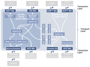
A network-on-chip interconnect with separate transaction, transport and physical layers (Source:Arteris)
Reading this article, you will be surprised like I was when you discover that the SoC interconnect did not receive the type of research and development focus that CPUs or GPUs received, and that as the SoC fabric became an afterthought in the design process, this critical component fell behind Moore’s Law. That sounds to me like testability was in the 1980’s, when the chip designer start thinking about Test when the chip design was almost completed. Then in the 1990’s, various techniques like Scan Test and Built-In Self Test (BIST) were developed by EDA vendors, and have since helped designers to focus on functional design, as soon as they follow a simple rule set. Nowadays, we could not imagine developing a SoC without automated Scan test and BIST.
In the same way, Kurt shows that NoC has been extensively used in highest growth segments in the industry, such as mobile application processors and LTE modems, and we can expect NoC to be much widely used during this decade, in SoC development addressing every industry segment, not only the very high volume Application Processor. What is the next step for NoC? Distributed cache coherent interconnects (CCI) fabrics will be the fourth era in the history of interconnects technology, according to Arteris. When should we expect cache coherent fabrics to become available available? That’s a good question we should ask to Arteris, as the company has become the undisputed leader of NoC IP…
Eric Esteve from IPNEST
lang: en_US


Comments
0 Replies to “History of SoC Interconnect Fabric”
You must register or log in to view/post comments.