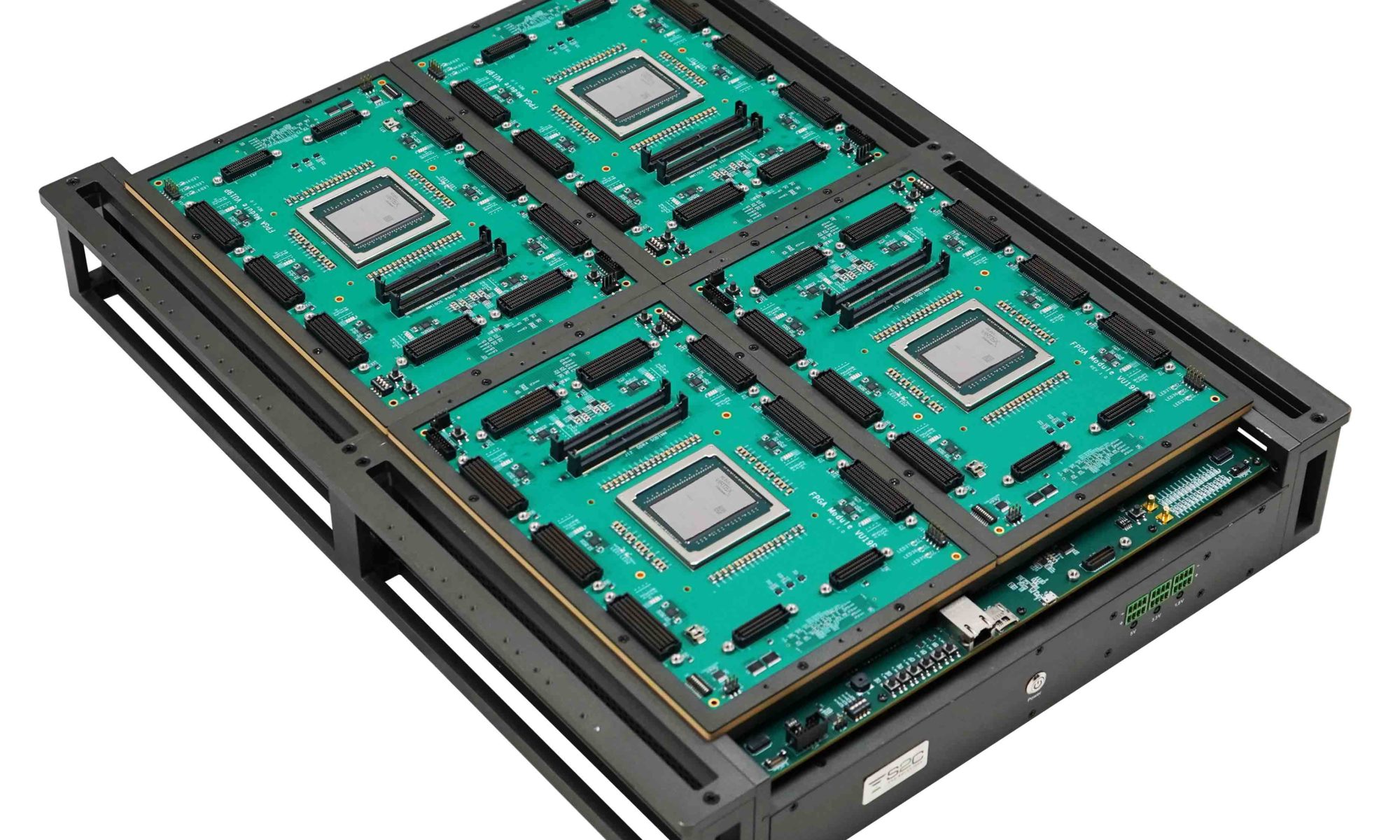

I was reading the S2C press release announcing their new FPGA prototyping platform based on the Xilinx UltraScale+ VU19P FPGA, and how the new FPGA will accelerate billion gate FPGA prototyping, and I was struck by the stunning implications of this announcement. Not that billion gate SoC designs can now be prototyped with FPGAs, the larger FPGA prototyping providers have been talking about this for a while. I was struck by the trajectory that FPGAs are on to hugely simplify FPGA prototyping. Twenty years ago, early FPGAs supported about 5K ASIC gates (Xilinx XC30902) and now the VU19P FPGA boasts an estimated 50M ASIC gates! That’s 10,000 times more ASIC gates from a single FPGA device in 20 years!

Request a Quote
Look, the biggest challenge for FPGA prototyping is getting an SoC design working in FPGAs fast. Not only to minimize the set-up effort of just one of the verification tools in the verification toolbox, but also to minimize the risk that the FPGA prototype never produces the expected pre-silicon verification ROI. Generally, bigger FPGAs reduces the number of FPGA devices needed to prototype an SoC design. The previous largest Xilinx FPGA, the UltraScale VU440, has an estimated capacity today of about 30M ASIC gates and it was announced in 2015.
If the new UltraScale+ VU19P delivers the expected 49M ASIC gate capacity, that’s 1.7 times more ASIC prototyping gates from a single FPGA in 5 years, and if the semiconductor industry is true to form, it’s not unreasonable to expect the FPGA gate capacity growth to be non-linear. So, simply using the same growth factor, it’s easy to project 80M ASIC gate FPGAs is less than 5 years, and 140M ASIC gate FPGAs is less than 10 years.
You can see where this thinking is going – we might be able to prototype a billion gate SoC design with 5 or 7 FPGAs in less than 10 years! Then, the job of getting an SoC design into an FPGA prototype will be super bigly simplified – or maybe just routine. The task of partitioning billion gate designs into multiple FPGAs gets much easier.
The prototype performance gets better because most of the interconnect would be contained within an FPGA. And, the cost of ownership should decline to the point where FPGA prototyping for large SoC designs approaches the pervasiveness that we see today for smaller SoC designs that fit into one or a few FPGAs.
If you are a skeptic, and are doubting that the FPGA companies can deliver on this aggressive capacity growth curve, take a look at the highly advanced packaging technology that Intel and Xilinx are using to produce their largest FPGAs today. The trending approach is to use logic fabric “chiplets” to increase yield on advanced silicon nodes and to reduce cost.
Combine this with 3D silicon interconnect, and heterogeneous die in the same package, and voila! – they could continue down this path all day long, possibly with a faster ASIC gate capacity growth factor than the last 5 years. As always, I’m betting on technology and a stellar future for FPGA prototyping.
Xilinx XC3000 FPGA Product Description
S2C Accelerates Billion Gate FPGA Prototyping with Xilinx Virtex UltraScale+ VU19P Based Systems
About S2C
S2C, is a global leader of FPGA prototyping solutions for today’s innovative SoC/ASIC designs. S2C has been successfully delivering rapid SoC prototyping solutions since 2003. With over 500 customers and more than 3,000 systems installed, our highly qualified engineering team and customer-centric sales team understands our users’ SoC development needs. S2C has offices and sales representatives in the US, Europe, Israel, China, Korea, Japan, and Taiwan. For more information please visit www.s2cinc.com.
Also Read:
S2C Announces 300 Million Gate Prototyping System with Intel® Stratix® 10 GX 10M FPGAs
Webinar: Hyperscale SoC Validation with Cloud-based Hardware Simulation Framework
WEBINAR: Prototyping With Intel’s New 80M Gate FPGA
Share this post via:


Comments
One Reply to “Prototyping with the Latest and Greatest Xilinx FPGAs”
You must register or log in to view/post comments.