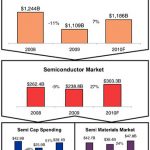
In a previous blog, Black Friday and the Predicted Semiconductor Shortages, I reported that total semiconductor manufacturing capacity is shrinking as older fabs close and new ones ramp up even slower than expected, resulting in a record reduction of total wafer capacity and silicon allocation starting in 2010. DRAM shortages… Read More
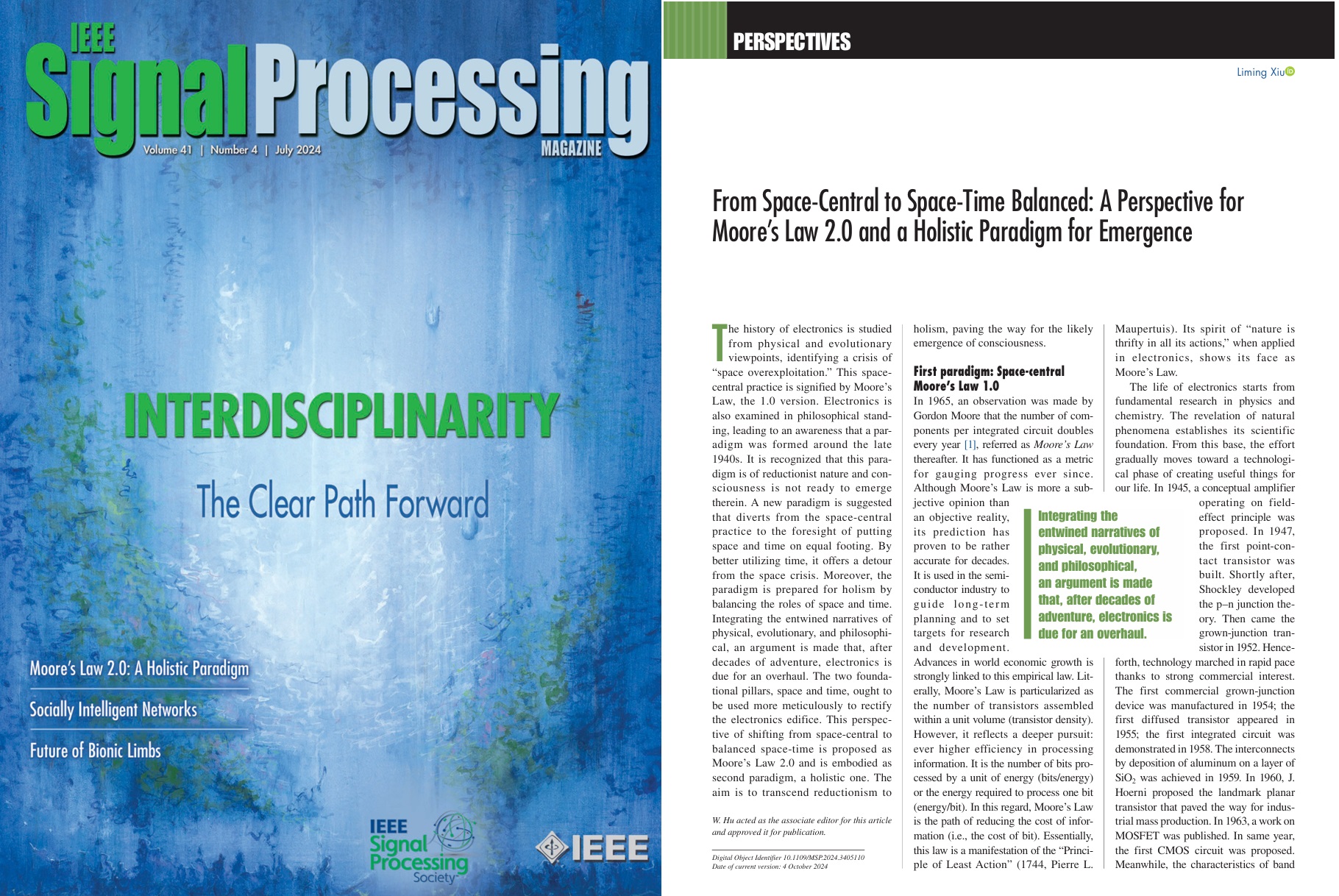 From Space-Central to Space-Time Balanced - A Perspective for Moore’s Law 2.0 and A Holistic Paradigm for EmergenceA friend of SemiWiki published an article on…Read More
 The RISC-V and Open-Source Functional Verification ChallengeMost of the RISC-V action at the end…Read More
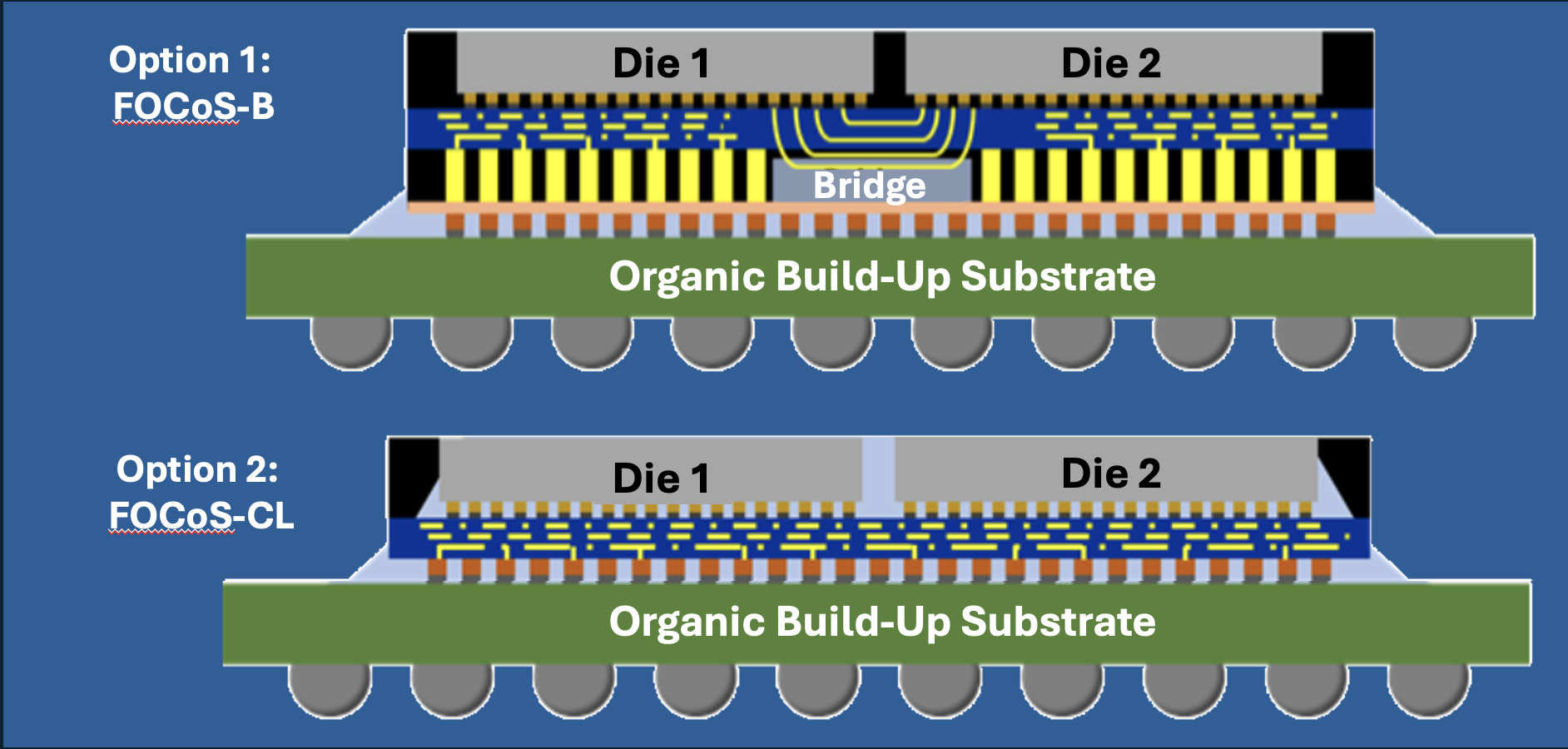 Sarcina Democratizes 2.5D Package Design with Bump Pitch Transformers2.5D package design is rapidly finding its stride…Read More
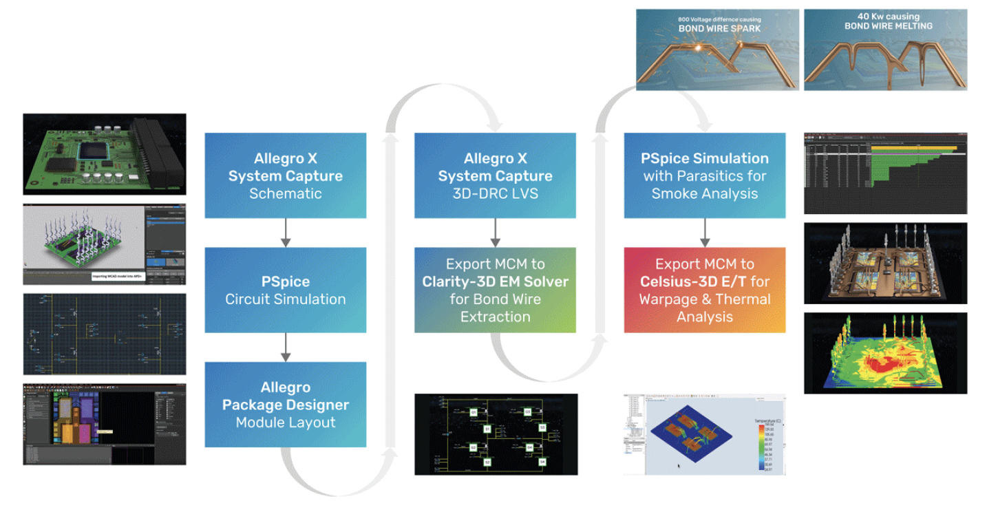 Addressing Reliability and Safety of Power Modules for Electric VehiclesAs electric vehicles (EVs) gain widespread adoption, safety,…Read More
TSMC OIP vs CDNS OIP Analysis
Launched in April 2008, the TSMC OIP initiative is a collaborative strategy aimed at breaking down the barriers of semiconductor design enablement in order to reduce waste and increase the profitability of the industry as a whole.
The TSMC Open Innovation Platform promotes timeliness-driven innovation amongst the semiconductor… Read More
450mm Semiconductor Manufacturing Debate
This blog posting is sponsored by EVA airlines, as I’m in the EVA executive lounge eating free food (I blog for food). “Fly EVA, the lesser of evils for Taiwan air travel!” EVA Air has a perfect safety record in 9 years of operation, China Air on the other hand has the worst safety record in the industry!
This blog was inspired by one of … Read More
2010 Semiconductor Foundry Update: Consolidation!
It has been an interesting month in the semiconductor business. Record revenues, profits, aggressive expansion plans, something we have not seen before and may not see again. Let’s start in Taiwan then move to Silicon Valley, Upstate New York, China, and Korea, with a look at: financials, capacity, and consolidation.
TSMC and… Read More
Cadence EDA360 Redux!
“Cadence Design Systems, Inc. (NASDAQ: CDNS), the global leader in EDA360………”
Of course, why wouldn’t Cadence be the global leader in something they just made up? As a follow-up to my yawningly successful blog Cadence EDA360 Manifesto:
One of the problems I have with EDA360 is the fear, uncertainty, and doubt (FUD) it attempts … Read More
Cadence EDA360 Manifesto
EDA360 is said to be a blueprint or high-level vision for the EDA industry and not a Cadence specific document, based on the challenges that customers are experiencing. What EDA36o really is, is a manifesto, a public declaration of intentions, opinions, objectives, or motives, issued by a specific organization. The question … Read More
Moore’s (Empirical Observation) Law!
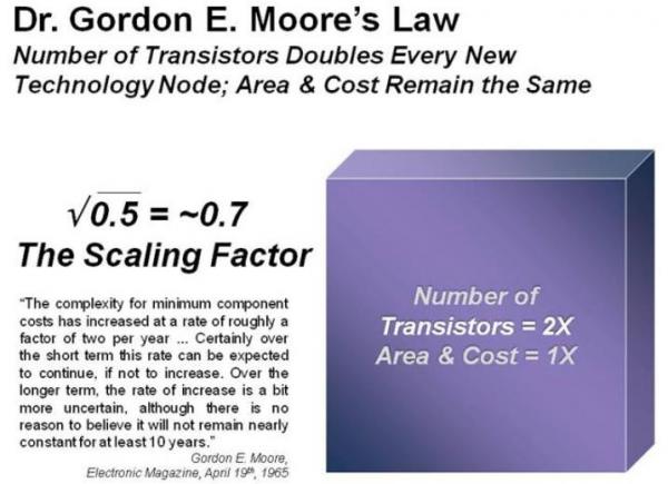
Moore slightly altered the formulation of the law over time, bolstering the perceived accuracy of Moore’s law in retrospect. Most notably, in 1975, Moore altered his projection to a doubling every two years. Despite popular… Read More
TSMC Earthquake Damage Redo
As you may know I enjoy poking fun at the current state of semiconductor design and manufacture media; sloppy reporting, editors with little or no actual semiconductor experience taking corporate marketing spins on news/events and passing it along as fact.
Last week it was the EETimes parroting the Samsung foundry business press… Read More
Redefining the Semiconductor Foundry Model: Abu Dhabi versus Taiwan
It was a pleasure to see the GlobalFoundries (GFI) corporate pitch at the Mentor Graphics U2U Conference last week. Wally Rhines is a tough act to follow but Mojy Chian, Senior Vice President of Design Enablement at GlobalFoundries, presented a compelling argument for a refined foundry business model. The GFI people were also … Read More
Redefining the Foundry Model: TSMC versus GlobalFoundries
The 17[SUP]th[/SUP] annual TSMC Technical Symposium finished its North American tour in Boston, a day before the Boston Marathon. I would like to be clever and say the foundry business is also a marathon but it clearly is not. If you watch TSMC, the foundry business is both a sprint AND a marathon!





AI Semiconductor Market