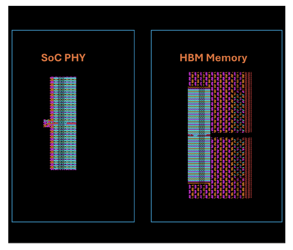
One of the challenges in doing a complex analog or mixed signal design is that things get out of step. One designer is tweaking the schematic and re-simulating, another is tweaking the layout of transistors, another is changing the routing. This is not because the design flow is messed up, but rather it reflects reality. If you wait… Read More
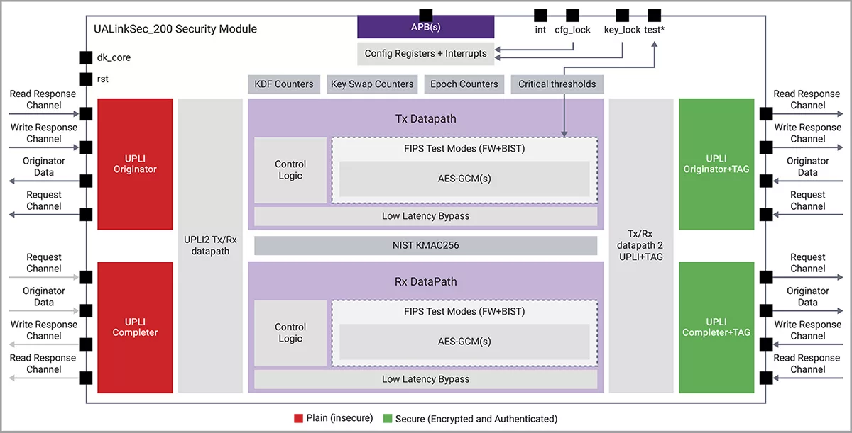
 Securing UALink in AI clusters with UALinkSec-compliant IPA classic networking problem is securing connections with…Read More
 Scaling Multi-Die Connectivity: Automated Routing for High-Speed InterfacesThis article concludes the three-part series examining key…Read More
 Arteris Highlights a Path to Scalable Multi-Die Systems at the Chiplet SummitAt the recent Chiplet Summit, presentations, discussions and…Read More
A Brief History of TSMC OIP
The history of TSMC and its Open Innovation Platform (OIP) is, like almost everything in semiconductors, driven by the economics of semiconductor manufacturing. Of course ICs started 50 years ago at Fairchild (very close to where Google is headquartered today, these things go in circles). The planarization approach, whereby… Read More
Reliability sign-off has several aspects – One Solution
Here, I am talking about reliability of chip design in the context of electrical effects, not external factors like cosmic rays. So, the electrical factors that could affect reliability of chips could be excessive power dissipation, noise, EM (Electromigration), ESD (Electrostatic Discharge), substrate noise coupling and… Read More
Real Heroes Don’t Wear Capes!
Real Heroes have many different jobs. My oldest son is a Math Teacher, he is a hero. You may have read about him before, he is the co-developer and administrator of SemiWiki. Think about it, without math where would the world be today?
My other son is a Fireman, Emergency Medical Technician, and also a hero. He is at the Rim Fire in Northern… Read More
OTP Memory to Build Smarter Power Management
All chips have critical power management requirements, often with multiple supply voltages. Digital power management ICs (PMICs) are commonplace to convert unregulated voltages from batteries and noisy power supplies to fully regulated accurate power to keep even the most sensitive chips performing.
Powervation is a company… Read More
Semiconductor Market Back to Healthy Growth
The worldwide semiconductor market is back to a healthy level of growth. WSTS data shows the 2Q 2013 global semiconductor market was up 6.0% from 1Q 2013 – the strongest quarter-to-quarter growth since 6.6% growth in 2Q 2011. Recent forecasts for 2013 market growth range from a conservative 2.1% from WSTS to an optimistic… Read More
Foundry 2.0: Why It Is Different And Why You Should Care
If you have been to an Ajit Manocha keynote recently, he talks a lot about Foundry 2.0. I covered his keynote at Semicon West in July here. Dan Hutcheson of VLSI Research interviewed Ajit about this new business model to identify it, see how it was different and see how GlobalFoundries were executing the model differently from the … Read More
Imagination Has More Stuff Than You…Imagine
Imagination seems to be well known for a couple of things. Firstly, everyone knows that it is the graphics processor used in the iPhone and the iPad and lots of other phones. And they know that Imagination acquired MIPS at the start of this year.
But what people don’t seem to really appreciate is just what a huge portfolio of IP… Read More
It’s a 14nm photomask, what could possibly go wrong?
Let’s start with the bottom line: in 14nm processes, errors which have typically been little more than noise with respect to photomask critical dimension (CD) control targets at larger process nodes are about to become very significant, even out of control if not accounted for.… Read More
FPGAs The Life Savers
Silicon dominates our lives, CPU’s, GPU’s are in the limelight but the unsung hero is the FPGA. They simply do the work where other silicon dare not tread, as they are unfit for the task. Never send a boy to do a man’s job.
For a moment, if we can, just for a few minutes perhaps we can break away from the social media bubble… Read More


Silicon Insurance: Why eFPGA is Cheaper Than a Respin — and Why It Matters in the Intel 18A Era