At the beginning of the year, New Delhi’s outgoing government launched an initiative purported to drive the nation’s technology independence and reduce the current account deficit on electronics imports. The initiative describes a partnership between New Delhi and two industrial consortiums for the building of semiconductor… Read More
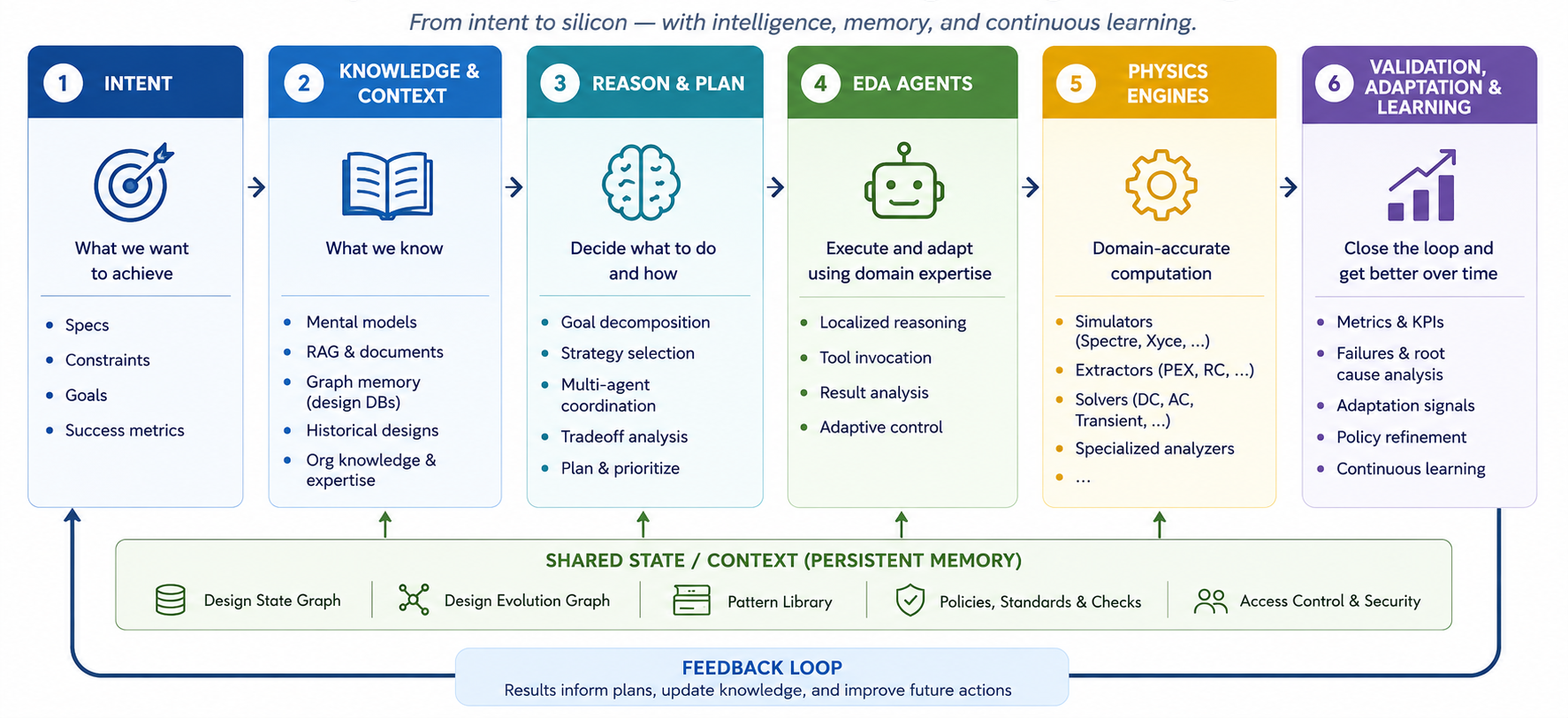 Beyond Workflow Agents: Toward Design Intelligence in Analog EDAOver the last year, the EDA industry has…Read More
 MooresLabAI at DAC 2026: Why the Future of Semiconductor Engineering Is Agentic, Not Just GenerativeFor decades, semiconductor innovation has been constrained not…Read More
 Caspia Technologies is pioneering a new, agentic chip and system security approach at DAC 2026Caspia’s advanced tools and agents blend seamlessly with…Read More
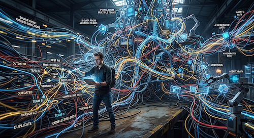 IP Lifecycle Management in the AI EraLarge design enterprises have multiple concurrent activities around…Read More
 See Autonomous Chip Design in Action with ChipAgents at DAC 2026Making the AI wave at DAC 2026 in…Read More
Sonics and Qualcomm Make a Deal
Some background. Sonics has been in the network-on-chip (NoC) business for a long time. Nearly 18 years years. When Arteris launched their products, Sonics figured Arteris were infringing Sonics’s patents and in 2011 brought a complaint against them. Details are here. Arteris looked at a couple of their own patents (if… Read More
The Great 28nm Debacle!
40nm was a big node while I was Director of Foundries at the IP company Virage Logic which was later acquired by Synopsys. 40nm was big because the top fabless companies multi-sourced designs from one foundry to another with relative ease to get the best wafer prices. It was also the node where some of the big IDMs went fab-lite moving… Read More
Coventor Brings More Accuracy & Performance into Design of MEMS Devices
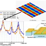
Although MEMS devices in various forms are now found in most electronic devices, predominantly in mobile, automotive, aerospace and many other applications, their major revolution, I believe, is yet to happen. We are seeing rapid innovation in MEMS reflected by their improvements in precision, performance, size reduction,… Read More
Fantasy Tech-Ball and the Intel Rumor Wire
Reading Intel analysis lately has been a lot like reading fantasy baseball analysis. Intel should buy Altera. Intel should waive Atom. Intel should fab for Apple. All of those have a near-zero probability of happening IMHO, and yet pundits continue to pitch their version of alternate reality, dealing away product lines and strategies… Read More
An Approach to Clock Domain Crossing for SoC Designs
Blogger Pawan Fangaria wrote about Clock Domain Crossing(CDC) a few weeks ago, and so I followed up tonight and watched a webinarabout CDC presented by Ravindra Anejaof Atrenta. An RTL design engineer would ultimately want a CDC verification tool that offers:
- Fast throughput and thoroughness
- Ability to debug and fix the source
Solar Leases, How to Not Get Gouged by PG&E
This post will be of primary interest to California residents.
If you haven’t looked closely at your PG&E bill, this may ruin your day. If you live in a house larger than a cracker box, and actually use your lights and air conditioning, the rates you pay are exorbitant. If you live in WA you’ll be paying .06-.08 per … Read More
July 4th Fireworks
It was July 4th yesterday. Fireworks. I didn’t go down to the waterfront to see them in San Francisco this year, I was in a “place” (that might possibly have served beer) having fun. But it reminded me of this a couple of years ago. On July 4th 2012 the San Diego fireworks display, one of the biggest in the world, detonated… Read More
Mentor Graphics @ SEMICON West 2014
Mentor is again the most represented EDA company at SEMICON West this year. I strongly advise Cadence and Synopsys to get more involved because EDA may be where electronics begins but semiconductor manufacturing makes all of our hard work come true, absolutely. Paul McLellan, Beth Martin, and I will be blogging live, I hope to see… Read More
GlobalFoundries Goes to Semicon West
Next week it is Semicon West, the big equipment vendor tradeshow. I love to go since EDA and semiconductor and all the stuff we are interested in here at Semiwiki are driven by equipment capabilities, especially lithography. The highest viewed blogs I write tend to be ones on technologies that are just a bit out beyond the stuff people… Read More
Consolidation and Competition: Who is Winning the $4.5 Billion Interface IP Race?