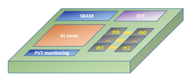


In today’s world where every device functions intelligently, it automatically becomes active on any kind of stimulus. The problem with such intelligence is that it can function unfavorably on any kind of bad stimulus. As the devices are complex enough in the form of SoCs (which at advanced process nodes are more susceptible to … Read More
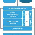
Ensuring Safety Distinctive Design & Verification


Musk’s Orbital Compute Vision: TERAFAB and the End of the Terrestrial Data Center