One of the most terrifying moments one can experience as a driver or passenger in a Tesla Model S driving with autopilot turned on is the realization that the system cannot recognize intersections or traffic lights. It seems like such a basic and obvious requirement for automated driving but the Model S can’t hack it –… Read More
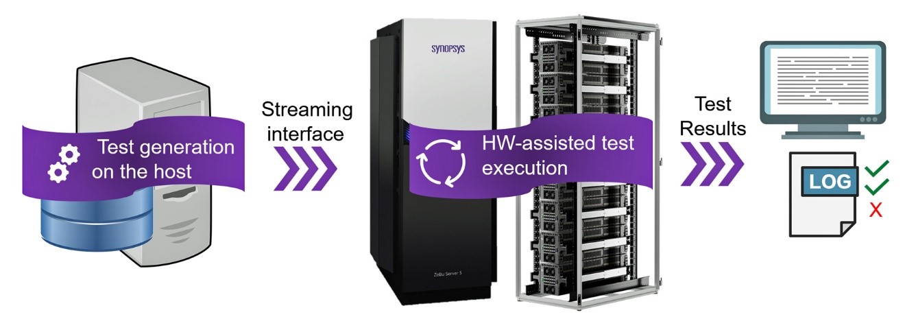 When Software Outruns Silicon: Hardware-Assisted Test Generation to the RescueFor the past decade, the semiconductor industry has…Read More
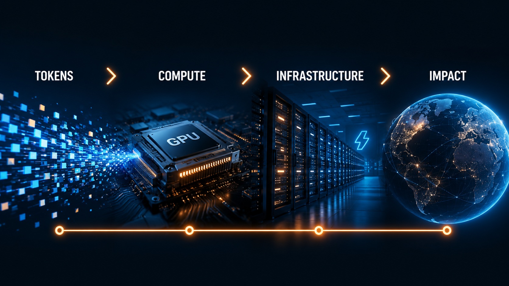 From Tokens to Infrastructure: Why Compute, Memory, and Power Will Determine the Future of AIBased on Dylan Patel’s SEMI Industry Strategy Symposium…Read More
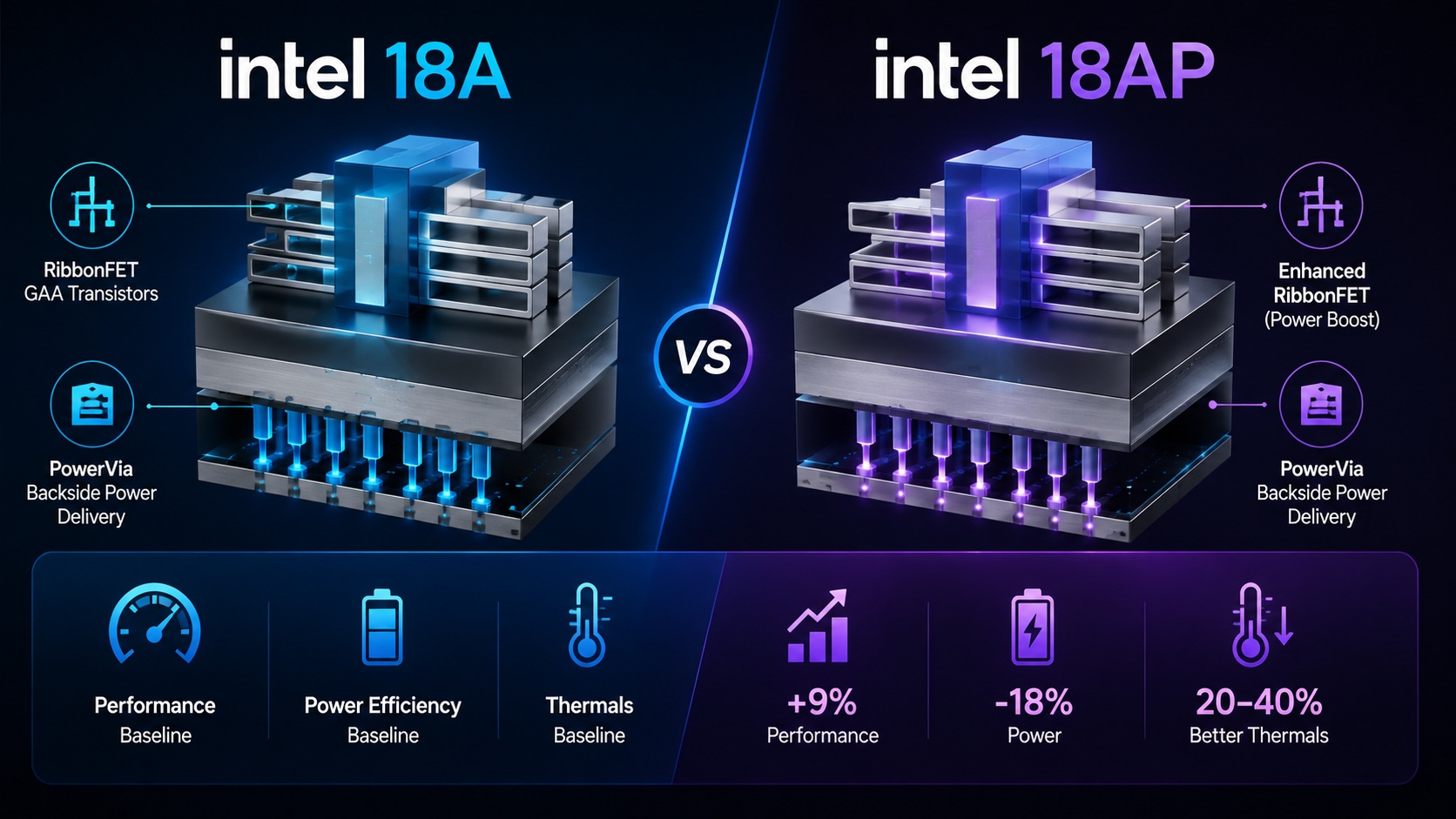 Intel 18A vs Intel 18A-P: What Is the Difference and Why Does It Matter?Intel’s 18A process technology has become one of…Read More
 WEBINAR: Why Google Cloud NetApp Volumes Matter for Modern EDA WorkloadsIn this webinar, Google Cloud and NetApp explore…Read More
 How to Free Yourself from Inconsistent Engineering Documentation Before It’s Too LateEmbedded systems programs often fail because critical engineering…Read More
Microsoft Raises The Mixed Reality Bar Yet Again With New Holographic Platform
There have been many hardware and software developments over the past 18 months in the worlds of AR and VR. However, most of them solely existed only within the separate realms of AR or VR. Many within the industry, including I, eventually see VR and AR merging into some hybrid reality that fluidly moves between the two. Some companies… Read More
Learn How to Debug UVM Test Benches Faster – Upcoming Synopsys Webinar

UVM for developing testbenches is a wonderful thing, as most verification engineers will attest. It provides abstraction capabilities, it encapsulates powerful operations, it simplifies and unifies constrained-random testing – it has really revolutionized the way we verify at the block and subsystem level.
However great… Read More
5 Reasons Why Platform Based Design Can Help Your Next SoC
Semiconductor design IP and verification IP have been around for decades, but just because your company has lots of IP doesn’t mean that you’re getting all of the benefits of a design reuse methodology. Maybe your business has encountered some of the following issues:
Android Auto-Rooting Malware – You Can Run But You Can’t Hide
There has been a startling rise in a class of Android auto-rooting malware which is believed to affect over a quarter of a million phones in the US and well over a million in each of India and China. The attack has primarily infected older versions of Android (so far) – KitKat, JellyBean and Lolipop primarily.
The malware, known as Shedun… Read More
Time-saving modules expand Prototype Ready family
A big advantage of FPGA-based prototyping is the ability to run real-world I/O at-speed, significantly faster and more accurately than hardware emulation systems typically requiring a protocol adapter. Dealing with real-world I/O means more thorough verification of SoC integration, and the opportunity to optimize systems… Read More
CEVA Launch CDNN2, Embedded Ready Neural Network
Convolutional Neural Network (CNN) recognition algorithm is generating very high interest in the semi industry. At first, because CNN provides best recognition quality when compared with alternative recognition algorithms. CEVA Deep Neural Network (CDNN) software framework, implemented with CEVA-XM4 imaging & vision… Read More
Data Analytics alone cannot deliver effective automation solutions for the industrial IOT
Automated analytics (which can also be referred to as machine learning, deep learning etc.) are currently attracting the lion’s share of interest from investors, consultants, journalists and executives looking at technologies that can deliver the business opportunities being afforded by the Internet of Things. The reason… Read More
APP ADD Will Cause the Next Tech Bust, Absolutely!
After playing Pokemon Go with my nephew this weekend I have another solid data point to support my hypothesis that we are in yet another tech boom. Let’s call it fad based investors jousting with unicorns. Think dotcom bubble of 2000. What drove the dotcom bubble? Cheap money, magical valuations, market overconfidence, and a good… Read More
Who Really Needs Intel’s New 10 Core, 20 Thread Broadwell-E Core i7 Processor?
At Computex 2016 in Taipei last week, Intel announced their newest lineup of processors which included a brand new 10-core Extreme Edition processor. The focal point of Intel’s new line-up of Broadwell-E processors, the successor to Intel’s previous Haswell-E workstation/enthusiast lineup is the 10-core Core i7-6950X. Intel… Read More
Why Huawei Says It Will Match TSMC’s Most Advanced Chips by 2031