I live in the future. I drive a Tesla electric vehicle, which controls the steering wheel on highways. My house in Menlo Park, Calif., is a “passive” home that expends minimal energy on heating or cooling. With the solar panels on my roof, my energy bills are close to zero — and that includes charging the car. My iPhone is encased in a … Read More
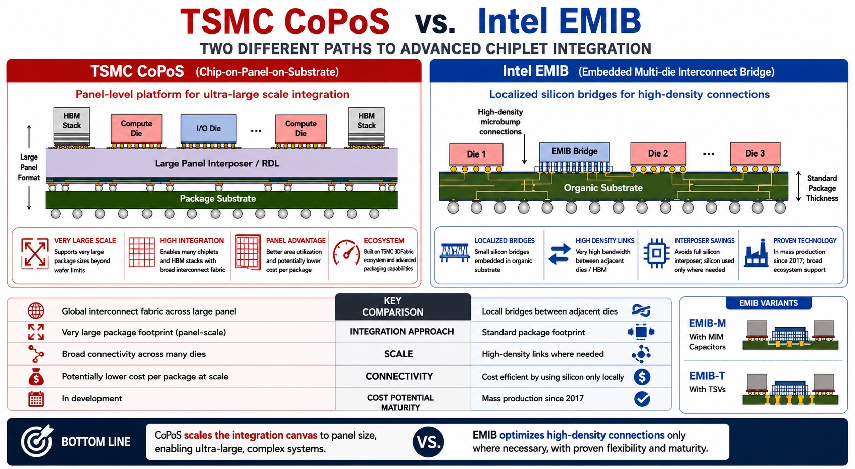 TSMC CoPoS Versus Intel EMIB Semiconductor PackagingTSMC’s CoPoS, generally described as Chip-on-Panel-on-Substrate, and Intel’s…Read More
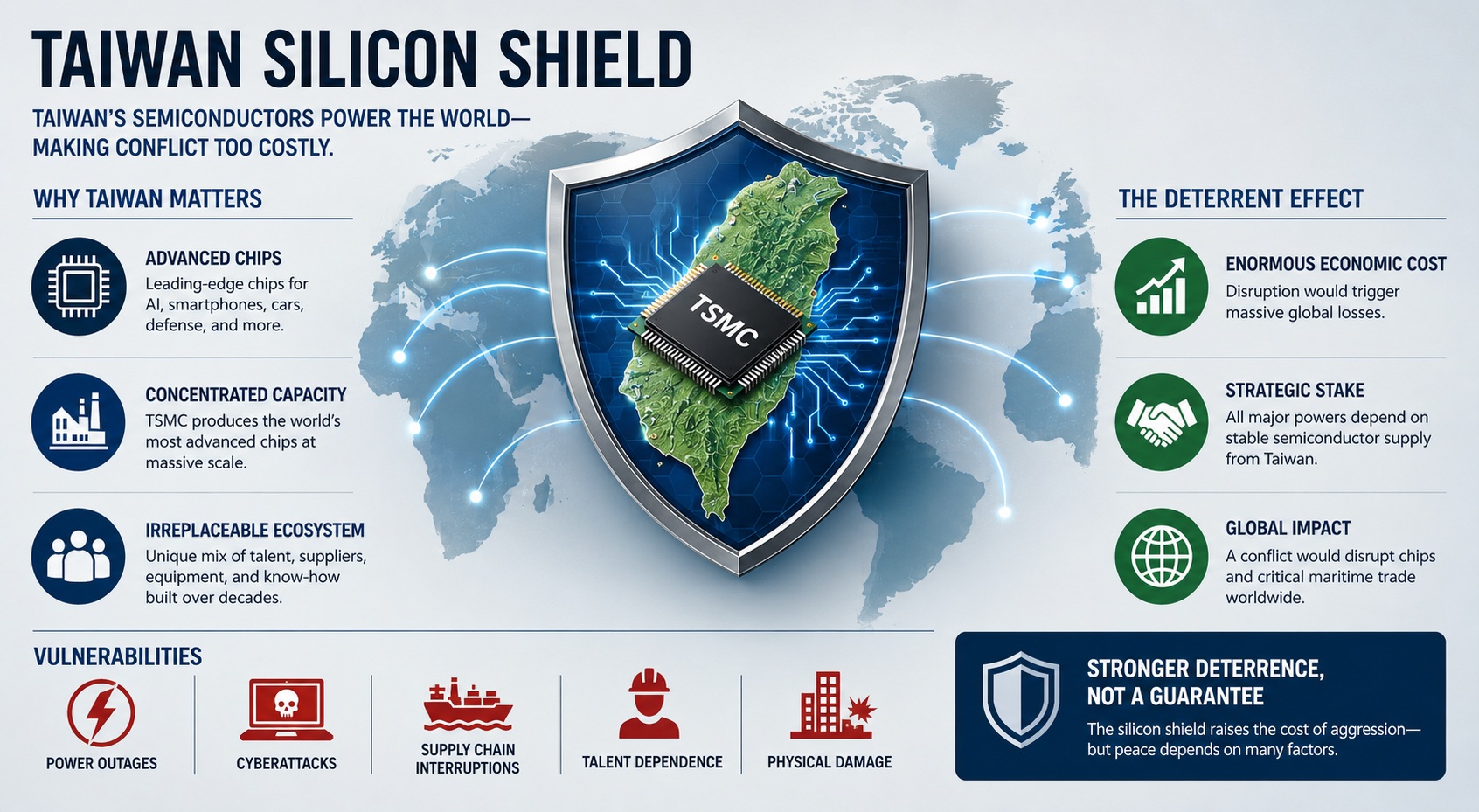 The Silicon Shield Has Never Been Stronger!The “Silicon Shield” describes the idea that Taiwan’s…Read More
 Agentrys Designs a Real Chip with its Multi-Agent WorkforceThe face of EDA is changing. For forty…Read More
 Must-See DAC Panel – Build vs Buy: Who Owns the Intelligence Behind Tomorrow's Chips?This year, DAC will be buzzing about AI…Read More
How Connected Healthcare is Becoming Vital
There is one word that describes the direction that the health care industry is heading, “connectivity”. This catch all term is used to describe using the internet to increase the reach of medicine. This is also known as the internet of things (IOT) and it is nothing new. It is however relatively new to healthcare.
The goal of connected… Read More
Pokemon Go’s Roots in Early Human Behavior
The popularity of Pokemon Go is really no mystery – it has its roots in our hunter gatherer evolution. Pokemon Go was an App that was just waiting to happen. It’s a perfect storm. It is the scavenger hunt brought into the modern age. But more importantly it recapitulates what our ancestors had to do to survive. It taps primal and… Read More
Keynote: Silicon is the New Steel: Building the World’s First Terascale Network
Prof. Thomas Lee from Stanford University is the keynote speaker at the upcoming 38th EOS/ESD Symposium (September 11-16, Anaheim). The EOS/ESD Symposium is focused on discussing the issues and providing the answers to electrostatic discharge in electronic production and assembly.
Abstract:
Steel transformed civilization… Read More
The Higgs Boson and Machine Learning
Technology in and around the LHC can sometimes be a useful exemplar for how technologies may evolve in the more mundane world of IoT devices, clouds and intelligent systems. I wrote recently on how LHC teams manage Big Data; here I want to look at how they use machine learning to study and reduce that data.
The reason high-energy physics… Read More
Webinar Alert – Helping Mixed Signal not be Mixed Up

Today’s profound statement: “don’t fall in love with your tools, figure out the biz process change first.” Mixed-signal SoC designers are having ample challenges with their design process and are in need of design management, but don’t want another tool to do it.… Read More
Apple, Alphabet, AT&T – We Have a Problem
Poor Dr. Sanjay Gupta, Emmy award-winning chief medical correspondent for CNN, a neurosurgeon and professor and now an explainer of distracted driving as part of CNN’s weeklong report on Driving While Distracted which concluded last Saturday. He offers a detailed medical explanation of driver distraction as only a neurosurgeon… Read More
Lam beats on EPS & Revs and good Q1 (Sept) guide
Continues to Outgrow in a Flat Capex Environment. Is September the 2016 Peak with a softer December? Lam reported June, Q4 , revenues of $1.55B and EPS of $1.80, handily beating estimates and besting relatively high expectations for a positive spin and outlook for H2. Guidance was for a Sept quarter of $1.625B in revs and $1.77 in … Read More
TSMC and Pokemon Go!
As Pokemon Go invades the world, let me give you a firsthand player’s description of the game and why the next generation of augmented reality apps will energize the fabless semiconductor ecosystem and greatly benefit TSMC.
While I am not a “gamer” per say, I am a technologist and am always looking for new semiconductor market drivers.… Read More
KLAC accelerates business into Q4 and where are we on the KLAM deal?
While no one was really paying attention, and the company didn’t have an earnings call anyway, KLAC put up a strong beat. Revenues came in at $919M versus street of $842M and EPS came in at $1.77 easily beating $1.42 street.
However this was at the expense of the September quarter as it appears that business in the September quarter… Read More
Enhancing Multi-Domain System Simulation with FMI Co-Simulation