You are currently viewing SemiWiki as a guest which gives you limited access to the site. To view blog comments and experience other SemiWiki features you must be a registered member. Registration is fast, simple, and absolutely free so please,
join our community today!
In 2015 we saw $85B in semiconductor acquisition activity and in 2016 there was more than $110B. Given 2015 and 2016 were relatively flat years for the $335B semiconductor industry and 2017 looks like more of the same we should expect consolidation to continue, absolutely.
So, let’s come up with a list of companies that may fall in… Read More
Bluetooth has always been a popular communication protocol for short-range applications, but now anticipating BT5 it’s really moving into the big leagues as a significant option for IoT applications. The new standard combines ultra-low power with significantly higher range and higher performance. Ultra-low power is always… Read More
I recently wrote an article about networks-on-chip (NoC) and how Systems-On-Chip integrated circuits (SoCs) are becoming increasingly more complex and heterogeneous in nature. While researching for that article I came upon a new micro-site by Dassault Systemes that goes into great detail about the operational challenges… Read More
Some companies are famously, even obsessively secretive about internal development. We never get to see discussion of areas they are working on (other than through patent filings) – we only see the polished and released product/service. Amazon is one such company but Apple must rank for many of us as the pre-eminent company in … Read More
The roster of automotive artificial intelligence (AI) initiatives is growing rapidly with Softbank working with Honda on the Emotion Engine for the Neuv self-driving commuter vehicle, IBM’s collaboration with General Motors and BMW, and, now, reports of Microsoft bringing AI to Volvo in the form of Cortana. It was Google… Read More
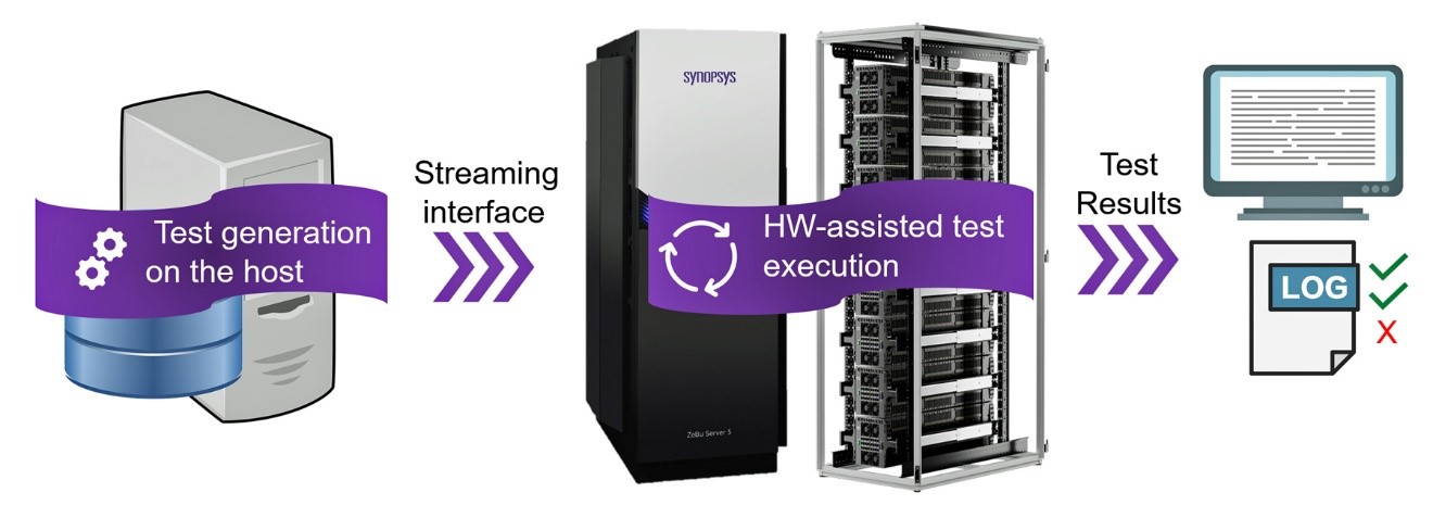
I attended a Mentor verification seminar earlier in the year at which Russ Klein presented a fascinating story about a real customer challenge in debugging a power problem in a design around an ARM cluster. Here’s the story in Russ’ own words. If you’re allergic to marketing stories, read it anyway. You might… Read More
Questions are being raised on how autonomous vehicles should react in life-or-death situations. Most of these have been based on thought experiments, constructed from standard dilemmas in ethics such as what should happen if the driver of a car or an autonomous car is faced with either killing two pedestrians or killing the occupants… Read More
Qualcomm was hit in December with a $853M fine by the Korea Fair Trade Commission (KFTC) for not fairly sharing patents related to mobile phone chipsets. In setting the standards for CDMA, WCDMA and LTE, agreements were struck that enable sharing technology to advance the standard. Fair, Reasonable and Non-Discriminatory (FRAND)… Read More
Joe has devoted his career to understanding and designing cache coherent systems and has been granted over 95 patents on the subject. For the past four years, he has been Chief Architect at NetSpeed, a developer of network-on-chip SoC interconnect.… Read More
If you are headed to Las Vegas for your New Year’s celebration, the annual Consumer Electronics Show or just a good time, beware! According to some estimates Nevada is the fourth most dangerous state for pedestrians and Las Vegas is ground zero for what the city calls an ePEDemic of roadway fatalities.
It’s difficult… Read More
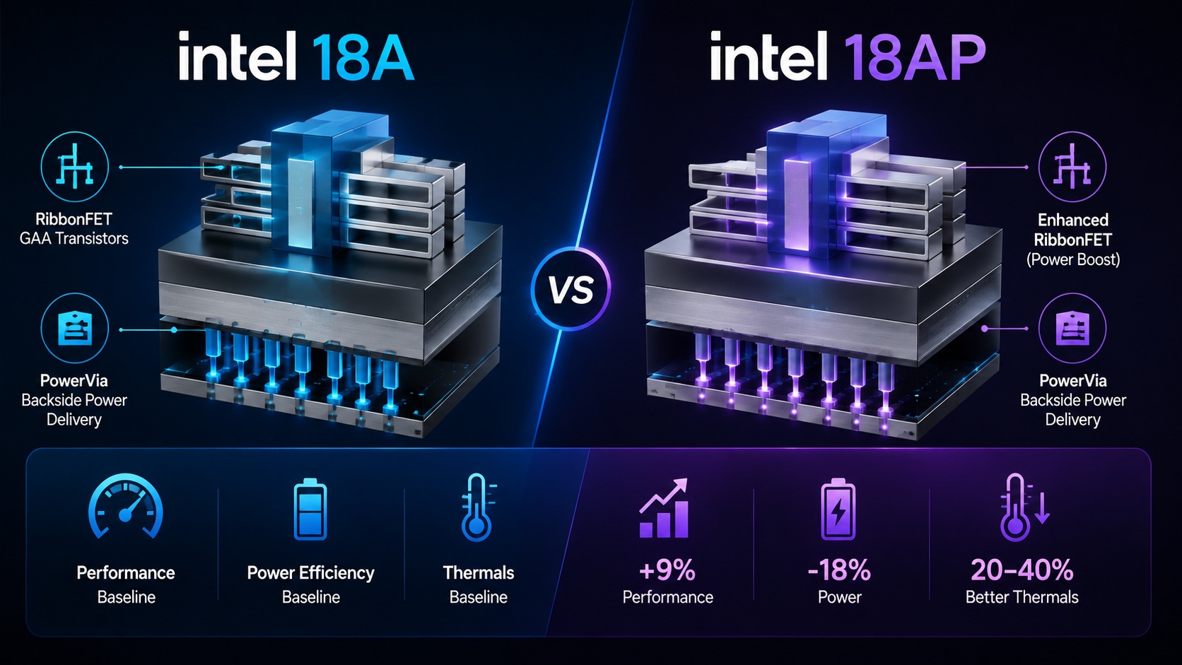


Intel 18A vs Intel 18A-P: What Is the Difference and Why Does It Matter?